CHESTER-X9
The CHESTER-X9 is a 4-channel low-side switch output module for the CHESTER platform.
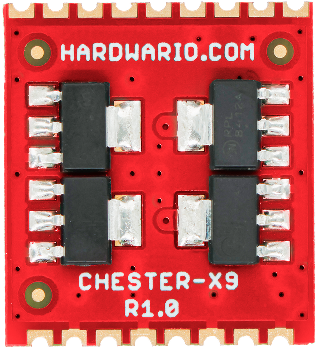
Module Overview
CHESTER-X9 switches up to four external loads to ground. Each channel is a self-protected NCV8412ASTT1G low-side switch (U1–U4): the channel output is pulled to GND when the channel is turned on, and left open (high-impedance) when it is off. Every channel is current-limited, so an overload or short circuit is contained without damaging the module.
Each switch is driven directly by one of the CHESTER-X GPIO pins (GP0–GP3). CHESTER-X9 has no I²C or SPI controller of its own. The load and its supply are entirely external: the load is wired between an external DC source (3–28 V) and a channel output, and the external source ground is tied to the module ground. The module does not supply power to the load or to the CHESTER mainboard.
Key Features
- 4 Independent Channels: Four low-side switches (CH1–CH4), each controlled separately.
- Self-Protected Switches: NCV8412ASTT1G with per-channel current limiting, thermal shutdown, and ESD protection.
- Integrated Inductive Clamp: Built-in drain-to-gate active clamp absorbs the turn-off energy of moderate inductive loads.
- Wide Load Voltage: External load supply from 3 to 28 VDC.
- Direct GPIO Control: Each channel is driven straight from a CHESTER-X GP pin, no I²C/SPI required.
- High Current: 2 A continuous and up to a 5 A current limit per channel.
Typical Applications
- Actuator & Relay Control: Switching relays, contactors, solenoids, and valves.
- Signalling: Driving lamps, beacons, and buzzers.
- Load Enable / Power Gating: Turning external DC loads on and off under firmware control.
- General Digital Outputs: Any low-side on/off output within the voltage and current limits.
Technical Specifications
| Parameter | Value |
|---|---|
| Module Type | 4-channel low-side switch output |
| Channels | 4 (CH1–CH4), independently controlled |
| Switch Device | NCV8412ASTT1G (one per channel) |
| Switching Type | Low-side (channel output switched to GND) |
| Load Supply Voltage | 3–28 VDC (external), per channel |
| Continuous Load Current | 2 A per channel |
| Peak Current Limit | 5 A per channel |
| Control | Direct GPIO (GP0–GP3) |
| Host Interface | None (no I²C/SPI device; direct GPIO control) |
| Board Interface | Castellated holes on two opposite edges, soldered to the CHESTER mainboard |
| Hardware Revision | R1.0 |
Key Components
| Component | Part Number | Description |
|---|---|---|
| Low-Side Switch (×4) | NCV8412ASTT1G | Self-protected low-side switch with current limiting, thermal shutdown, integrated inductive clamp, and ESD protection; one per channel |
Pin Configuration
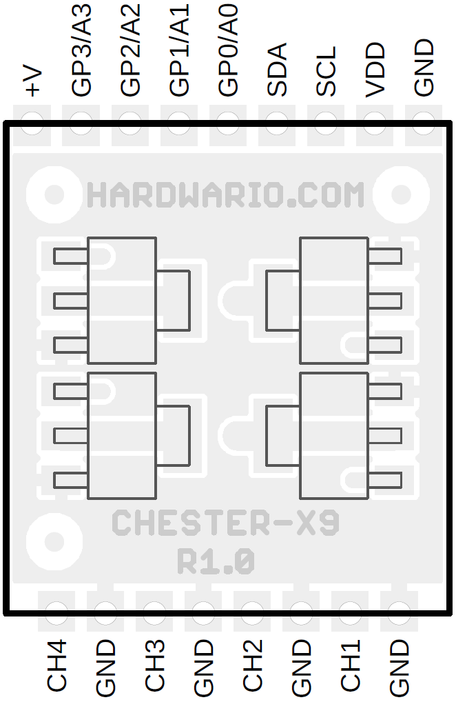
The module uses a standardized header layout compatible with CHESTER extension slots.
The pin configuration shown is for the CHESTER-M CGLS mainboard.
CHESTER-X9 Connector Pinout
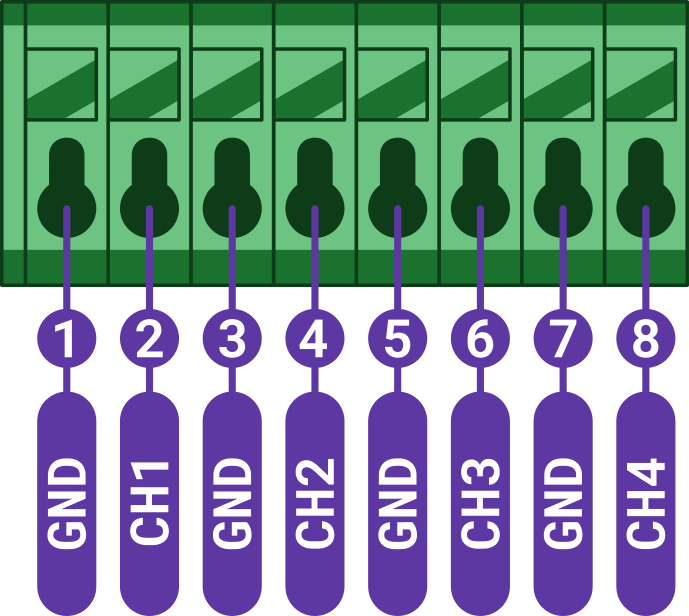
| Pin | Signal | Type | Description |
|---|---|---|---|
| 1 | GND | Ground | System ground / external-source return |
| 2 | CH1 | Switch Output | Channel 1 low-side switch output |
| 3 | GND | Ground | System ground / external-source return |
| 4 | CH2 | Switch Output | Channel 2 low-side switch output |
| 5 | GND | Ground | System ground / external-source return |
| 6 | CH3 | Switch Output | Channel 3 low-side switch output |
| 7 | GND | Ground | System ground / external-source return |
| 8 | CH4 | Switch Output | Channel 4 low-side switch output |
CHESTER-X9 does not power the load or the CHESTER mainboard. Each channel only switches its output to GND; the load is powered from an external 3–28 VDC source (see Switch and Load Connection below).
Channel Control (GPIO)
Unlike most CHESTER-X modules (which use I²C or SPI), CHESTER-X9 is controlled directly through the module slot's GPIO pins. Each GP pin drives the gate of one low-side switch, so asserting a GP pin turns that channel on (connects its output to GND):
| CHESTER-X pin | Channel | Switch | Schematic net |
|---|---|---|---|
| GP0 / A0 | CH1 | U1 | OUT0 |
| GP1 / A1 | CH2 | U2 | OUT1 |
| GP2 / A2 | CH3 | U3 | OUT2 |
| GP3 / A3 | CH4 | U4 | OUT3 |
The slot also carries the I²C bus (SDA/SCL), but CHESTER-X9 uses no I²C device. All four channels are switched by the GP pins alone.
Switch and Load Connection
Each load is wired between the external DC source (+) and a channel output (CH1–CH4); the channel's low-side switch then completes the circuit to GND when it is turned on. The external source ground must be connected to one of the module's GND terminals so the module and the external supply share a common ground reference.
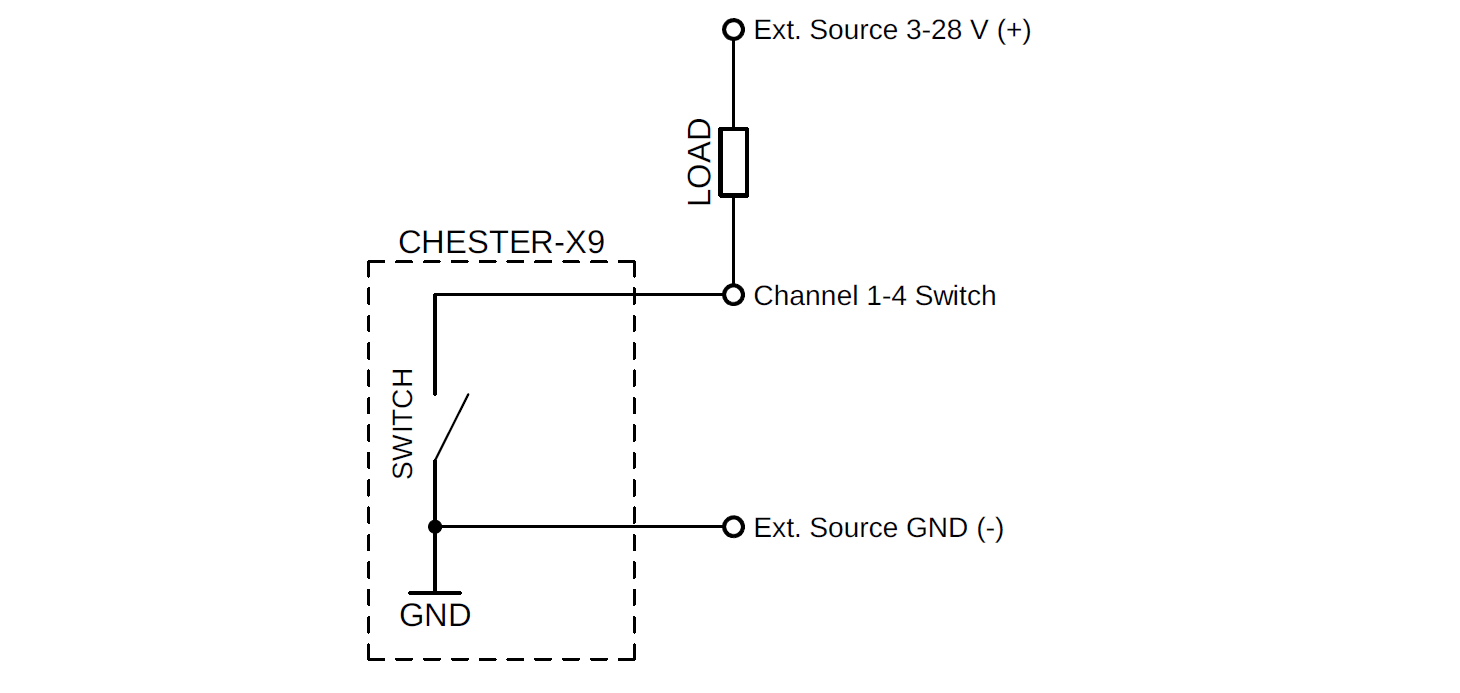
CHESTER-X9 has no external freewheeling (flyback) diode. The NCV8412ASTT1G integrates a drain-to-gate active clamp that absorbs the turn-off energy of moderate inductive loads (small relays, solenoids, valves), so they can be switched directly. For large inductances, high currents, or fast repetitive switching, add an external freewheeling diode across the load to keep the switch within its clamp-energy rating.
Enclosure Feed-Through
Two options bring the load cable into the enclosure:
- Cable gland (default): route the load conductors through a cable gland in the enclosure wall and wire them to the terminal block.
- Panel-mount connector (on request): an external connector in the enclosure wall lets the user plug in the load cable, with no loose wiring inside. Available on request.
Compatible CHESTER Configurations
The CHESTER-X9 module can be used with various CHESTER mainboard configurations. Below are examples of compatible setups:
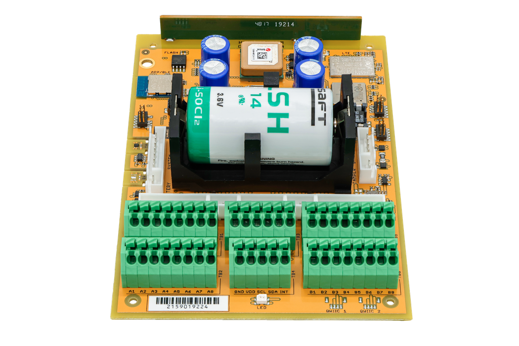
CHESTER-M (CGLS)
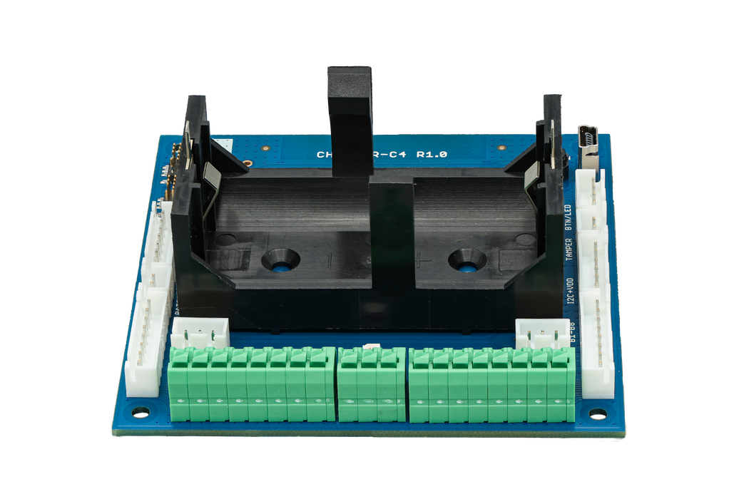
CHESTER-C4
CHESTER SDK usage
CHESTER-X9 can be used as part of the CHESTER SDK using the ctr_x9_a and ctr_x9_b shields, or hardware-chester-x9-a and hardware-chester-x9-b Project Generator features.
Schematic Diagrams
The complete schematic, showing the four NCV8412ASTT1G low-side switches and the connector mapping, is available as a PDF:
Module Drawing