CHESTER-X7
The CHESTER-X7 is an analog input extension module for the CHESTER platform, with one differential input, one single-ended voltage input, and a 5 V output to power external probes.
Module Overview
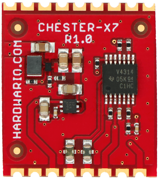
CHESTER-X7 provides a differential input (INP/INM) for current probes and other industrial sensors, and a single-ended voltage input (VIN) for 0–28 V signals. The differential input is buffered by precision zero-drift op-amp stages (OPA4387) and presented to the CHESTER analog inputs (INP → A0, INM → A1). The voltage input is scaled by a precision resistor divider and read on A2. CHESTER-X7 has no I²C or SPI interface — all three signals are read directly by the CHESTER mainboard's ADC.
The module also generates a regulated 5.0 V output (VOUT) to power the connected probes. It is produced from the +V rail by a boost converter (TPS61099) followed by a low-noise LDO (TPS7A2050), and is enabled under firmware control through the slot's GP3/A3 pin, so probe power can be switched off between measurements to save energy.
Key Features
- Differential Input: One differential input (INP/INM) for current probes and industrial sensors, buffered by precision OPA4387 op-amp stages.
- Voltage Input: One single-ended 0–28 V input (VIN), precision-divided for the CHESTER ADC.
- Analog Interface: Signals are read directly on the CHESTER analog inputs (A0/A1/A2) — no I²C or SPI needed.
- Switchable Probe Power: Regulated 5.0 V output (VOUT) to power the probes, enabled via GP3/A3.
- Precision Analog: Zero-drift OPA4387 op-amp and 0.1% resistors for accurate, low-drift measurements.
Typical Applications
- Current Measurement: Reading current probes, current transformers (CTs), and shunt-based current sensors.
- Industrial Sensor Interfacing: Differential sensors and transducers that need a powered, buffered front-end.
- Voltage Monitoring: Measuring DC voltages up to 28 V — battery banks, supply rails, and industrial signals.
- Process & Energy Monitoring: Load, power, and consumption monitoring in industrial and building systems.
- Analog Signal Acquisition: General-purpose acquisition of low-level differential or single-ended signals.
Technical Specifications
| Parameter | Value |
|---|---|
| Module Type | Analog input front-end (differential + voltage) |
| Differential Input | INP/INM, buffered by OPA4387, read on A0/A1 |
| Voltage Input (VIN) | 0–28 V single-ended, precision-divided, read on A2 |
| Probe Power Output (VOUT) | Regulated 5.0 V (boost + LDO), enabled via GP3/A3 |
| Host Interface | Analog (CHESTER ADC on A0/A1/A2); no I²C/SPI |
| Control | GP3/A3 enables the 5.0 V probe-power output |
| Logic Supply (VDD) | 3.0 V |
| Board Interface | Castellated holes on two opposite edges, soldered to the CHESTER mainboard |
| Hardware Revision | R2.1 |
Key Components
| Component | Part Number | Description |
|---|---|---|
| Boost Converter | TPS61099YFF | Step-up converter generating the intermediate 5.5 V rail from +V |
| LDO Regulator | TPS7A2050PDBVR | Low-noise 5.0 V LDO producing the VOUT probe supply |
| Precision Op-Amp | OPA4387PW | Zero-drift quad op-amp buffering the differential input |
Pin Configuration
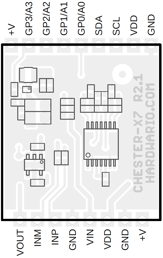
The module uses a standardized header layout compatible with CHESTER extension slots.
The pin configuration shown is for the CHESTER-M CGLS mainboard.
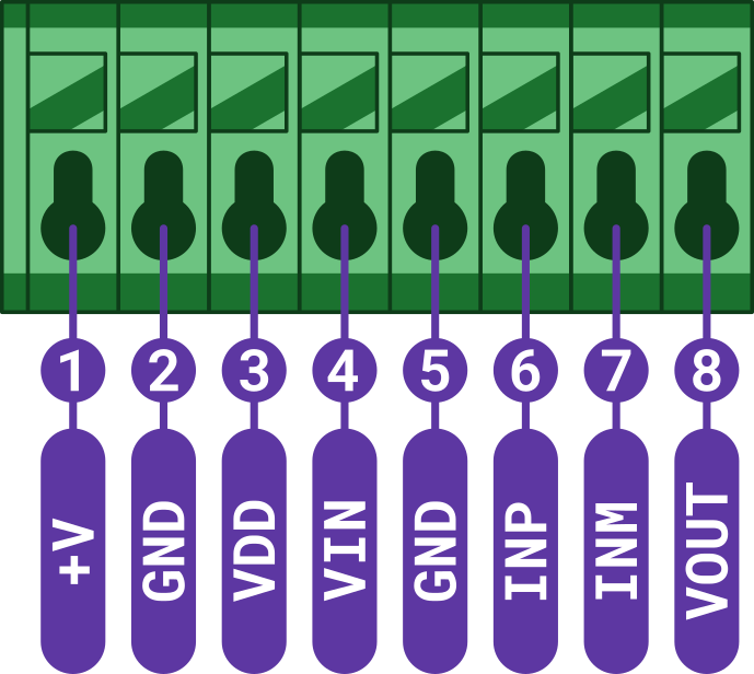
CHESTER-X7 Connector Pinout
| Pin | Signal | Type | Description |
|---|---|---|---|
| 1 | +V | Power | System positive rail (depends on the CHESTER power-supply option); also feeds the boost converter |
| 2 | GND | Ground | System ground reference |
| 3 | VDD | Power | 3.0 V logic supply from the CHESTER mainboard |
| 4 | VIN | Analog Input | Single-ended voltage input (0–28 V) |
| 5 | GND | Ground | System ground reference |
| 6 | INP | Analog Input | Positive differential input |
| 7 | INM | Analog Input | Negative differential input |
| 8 | VOUT | Power Output | Regulated 5.0 V probe-power output |
VDD is the 3.0 V logic rail and +V is the system positive rail (its voltage depends on the CHESTER power-supply option; it also feeds the on-board boost converter). VOUT provides a regulated 5.0 V to power the connected probes and is enabled from firmware via GP3/A3.
Signal Routing (Analog)
CHESTER-X7 has no I²C or SPI device — the measurements are read directly on the CHESTER analog inputs, and one GP pin switches the probe power. The slot pins are used as follows:
| CHESTER-X pin | Direction | Function |
|---|---|---|
| GP0 / A0 | Analog in | Buffered positive differential input (INP) |
| GP1 / A1 | Analog in | Buffered negative differential input (INM) |
| GP2 / A2 | Analog in | Scaled voltage input (VIN, 0–28 V) |
| GP3 / A3 | Digital out | Enables the 5.0 V probe-power output (VOUT) |
The differential input legs (INP, INM) are each buffered by a precision OPA4387 stage and read on A0 and A1; firmware takes their difference. The voltage input (VIN) is divided by a precision resistor network and read on A2. The slot's I²C bus (SDA/SCL) is not used.
Input and Output Connection
- Current probe / differential sensor: connect the probe's differential output to INP (pin 6) and INM (pin 7). If the probe needs power, take it from VOUT (pin 8, 5.0 V) and GND.
- Voltage input: connect the 0–28 V source to VIN (pin 4) and GND.
All externally connected devices must share a common GND with the module. Enable the 5.0 V probe supply from firmware (GP3/A3) before taking a measurement.
Enclosure Feed-Through
Two options bring the wiring into the enclosure:
- Cable gland (default): route the conductors through a cable gland in the enclosure wall and wire them to the terminal block.
- Panel-mount connector (on request): an external connector in the enclosure wall lets the user plug in the cable, with no loose wiring inside. Available on request.
Compatible CHESTER Configurations
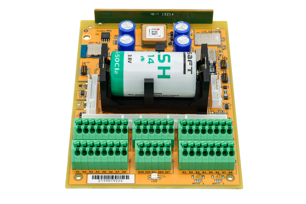
The CHESTER-X7 module can be used with various CHESTER mainboard configurations. Below are examples of compatible setups:
CHESTER-M (CGLS)
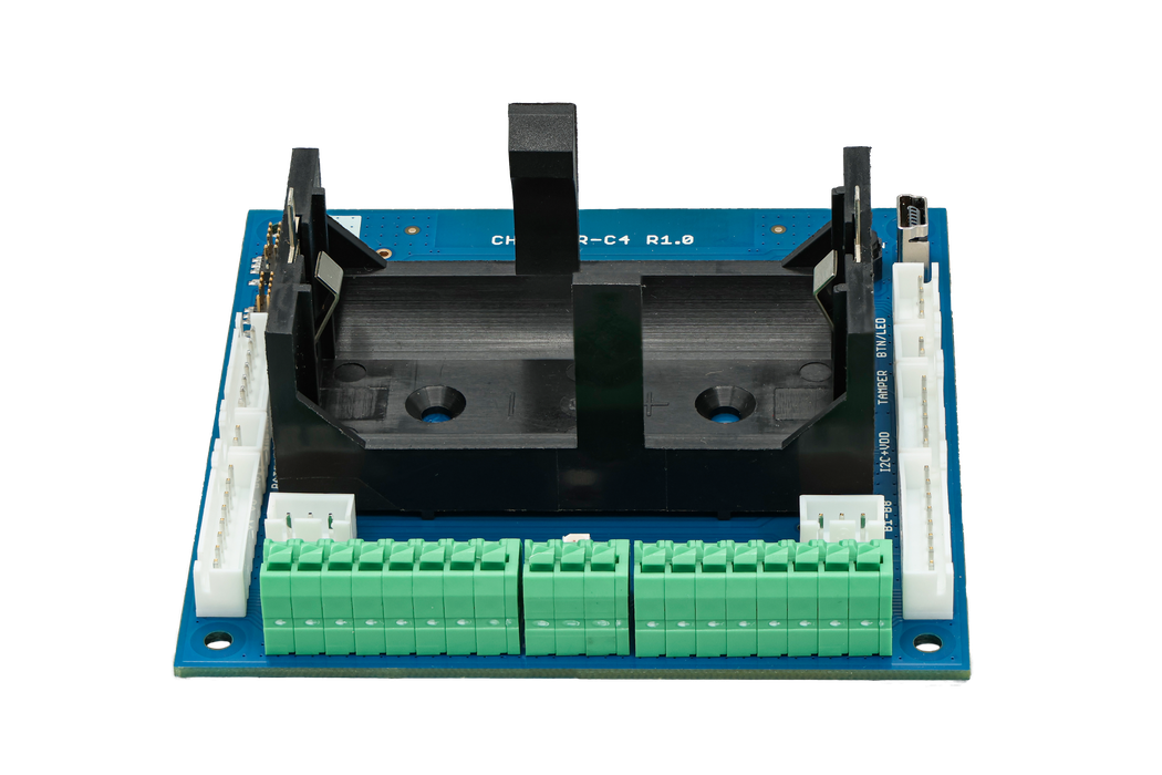
CHESTER-C4
CHESTER SDK usage
CHESTER-X7 can be used as part of the CHESTER SDK using the ctr_x7_a and ctr_x7_b shields, or hardware-chester-x7-a and hardware-chester-x7-b Project Generator features.
Schematic Diagrams
The complete schematic — the boost/LDO probe-power supply and the differential/voltage input front-end — is available as a PDF:
Module Drawing