CHESTER-X8
The CHESTER-X8 is a precision 3-axis accelerometer extension module for the CHESTER platform.
Module Overview
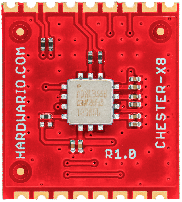
CHESTER-X8 measures acceleration on three axes with the ADXL355 low-noise, low-drift MEMS accelerometer. It offers selectable ±2 g / ±4 g / ±8 g ranges and a resolution of up to 3.9 μg/LSB (at the ±2 g range), with a low zero-g offset. The ADXL355 connects to the CHESTER mainboard over I²C at the fixed address 0x1D; its two interrupt outputs (INT1, INT2) are routed to the slot's GP0 and GP1 pins.
In addition to the on-board accelerometer, the module's terminal block breaks out the I²C bus (SCL/SDA), two user GPIO lines (DIO1, DIO2), and the power rails (VDD 3.0 V, +V, GND). This lets you attach external I²C devices on the same bus or use the two GPIO lines directly. The module has no on-board voltage regulator. It runs from the CHESTER rails.
Key Features
- Precision 3-Axis Accelerometer: ADXL355 low-noise, low-drift MEMS sensor.
- Selectable Ranges: ±2 g, ±4 g, and ±8 g.
- High Resolution: Up to 3.9 μg/LSB (at the ±2 g range), with a low zero-g offset.
- I²C Interface: Fixed address 0x1D, with two interrupt lines routed to GP0 and GP1.
- I²C & GPIO Breakout: The terminal block exposes the I²C bus, two GPIO (DIO1/DIO2), and power for expansion.
- No External Supply Needed: Runs directly from the CHESTER rails (VDD 3.0 V).
Typical Applications
- Tilt & Inclination Sensing: Measuring angle and orientation.
- Vibration Monitoring: Detecting and characterizing vibration.
- Structural Health Monitoring: Tracking movement or settling of structures.
- Machine Condition Monitoring: Watching rotating and reciprocating equipment.
- Seismic & Geotechnical Sensing: Capturing low-amplitude, low-frequency motion.
- Tamper & Movement Detection: Detecting manipulation or movement of the device and its carrier board.
Technical Specifications
| Parameter | Value |
|---|---|
| Module Type | Precision 3-axis accelerometer |
| Accelerometer | ADXL355 (3-axis MEMS) |
| Measurement Ranges | ±2 g, ±4 g, ±8 g |
| Resolution | Up to 3.9 μg/LSB (at the ±2 g range) |
| Host Interface | I²C |
| I²C Address | 0x1D (fixed; ASEL tied low) |
| Interrupt Lines | INT1 → GP0/A0, INT2 → GP1/A1 |
| User Digital I/O | DIO1 (GP2/A2), DIO2 (GP3/A3), on the terminal block |
| Logic Supply (VDD) | 3.0 V |
| Board Interface | Castellated holes on two opposite edges, soldered to the CHESTER mainboard |
| Hardware Revision | R1.0 |
Key Components
| Component | Part Number | Description |
|---|---|---|
| Accelerometer | ADXL355 | Low-noise, low-drift 3-axis MEMS accelerometer with a digital interface (used here in I²C mode) |
Pin Configuration
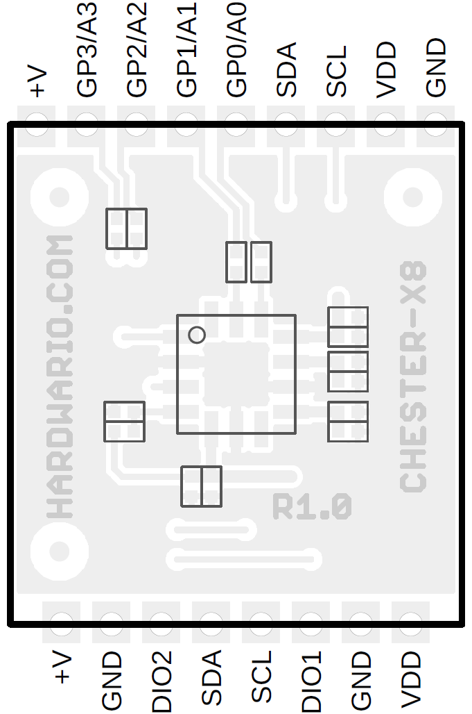
The module uses a standardized header layout compatible with CHESTER extension slots.
The pin configuration shown is for the CHESTER-M CGLS mainboard.
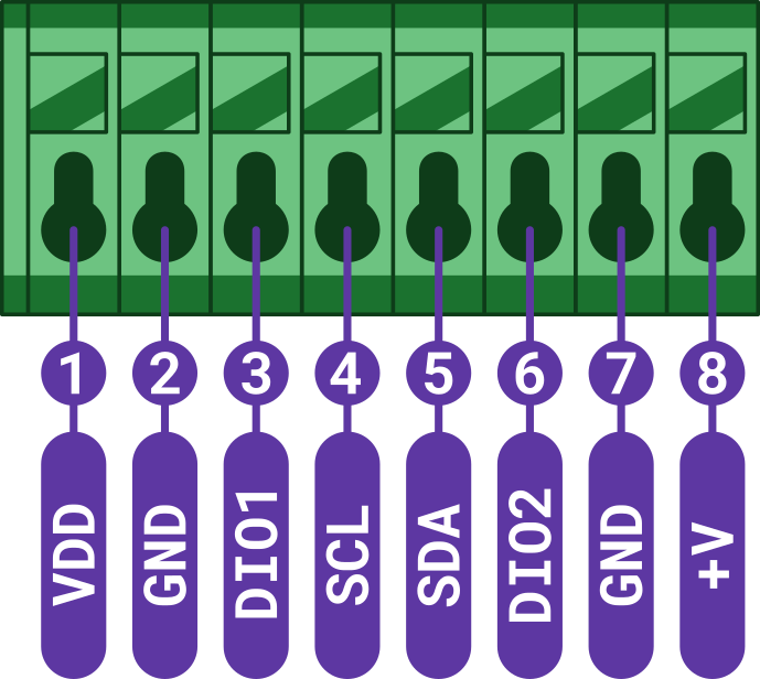
CHESTER-X8 Connector Pinout
| Pin | Signal | Type | Description |
|---|---|---|---|
| 1 | VDD | Power | 3.0 V logic supply from the CHESTER mainboard |
| 2 | GND | Ground | System ground reference |
| 3 | DIO1 | Digital I/O | User digital input/output #1 (slot GP2/A2) |
| 4 | SCL | I²C | I²C clock |
| 5 | SDA | I²C | I²C data |
| 6 | DIO2 | Digital I/O | User digital input/output #2 (slot GP3/A3) |
| 7 | GND | Ground | System ground reference |
| 8 | +V | Power | System positive rail (depends on the CHESTER power-supply option) |
VDD is the 3.0 V logic rail; +V is the system positive rail and its voltage depends on the CHESTER power-supply option. Besides powering the on-board ADXL355, the terminal block also breaks out the I²C bus (SCL/SDA) and two user GPIO (DIO1, DIO2) for expansion.
Host Interface (I²C)
CHESTER-X8 communicates with the CHESTER mainboard over the standard I²C bus. The on-board ADXL355 accelerometer sits at the fixed I²C address 0x1D (the ASEL strap is tied low). The same I²C bus is exposed on the terminal block (SCL/SDA), so external I²C devices can share it. Just avoid a second device at address 0x1D.
The module uses the slot's GP pins as follows:
| CHESTER-X pin | Function | Connected to |
|---|---|---|
| GP0 / A0 | ADXL355 INT1 | Accelerometer interrupt 1 |
| GP1 / A1 | ADXL355 INT2 | Accelerometer interrupt 2 |
| GP2 / A2 | DIO1 | User GPIO (terminal block) |
| GP3 / A3 | DIO2 | User GPIO (terminal block) |
The ADXL355 data-ready output (DRDY) is not brought out; use the INT1/INT2 lines (GP0/GP1) for interrupt-driven sampling.
Terminal Block and Expansion
Besides carrying the on-board accelerometer, the terminal block breaks out the I²C bus, two GPIO lines, and the power rails, so CHESTER-X8 can also serve as a small expansion header:
- External I²C devices: wire them to SCL (pin 4), SDA (pin 5), VDD (pin 1, 3.0 V), and GND (pin 2 or 7). They share the bus with the on-board ADXL355 (address 0x1D).
- User GPIO: DIO1 (pin 3) and DIO2 (pin 6) are the slot's GP2/GP3 lines, usable as general digital inputs or outputs.
- Power: +V (pin 8) is the system positive rail; VDD (pin 1) is the 3.0 V logic rail.
All externally connected devices must share a common GND with the module.
Enclosure Feed-Through
Two options bring the wiring into the enclosure:
- Cable gland (default): route the conductors through a cable gland in the enclosure wall and wire them to the terminal block.
- Panel-mount connector (on request): an external connector in the enclosure wall lets the user plug in the cable, with no loose wiring inside. Available on request.
Compatible CHESTER Configurations
The CHESTER-X8 module can be used with various CHESTER mainboard configurations. Below are examples of compatible setups:
CHESTER-M (CGLS)
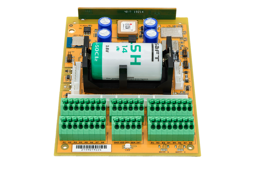
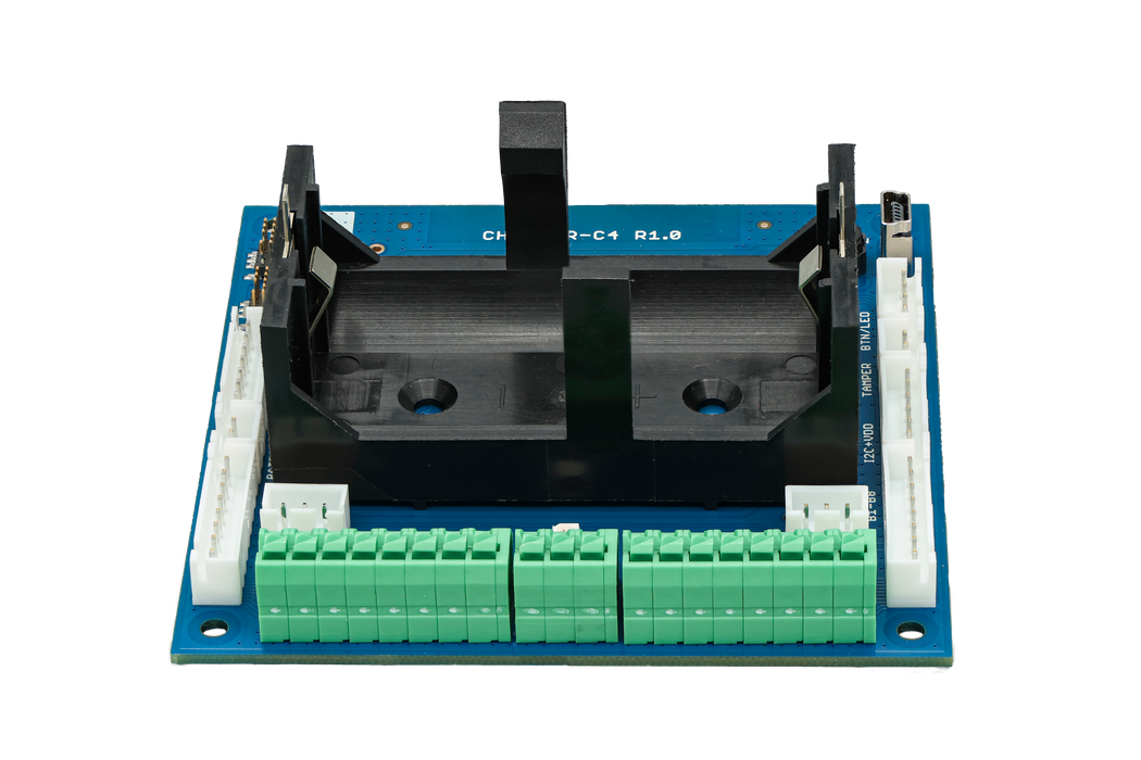
CHESTER-C4
Schematic Diagrams
The complete schematic, showing the ADXL355 accelerometer, its I²C interface and interrupt routing, and the terminal-block breakout, is available as a PDF:
Module Drawing