CHESTER-C5
This article describes the CHESTER-C5 carrier board.
Module Overview
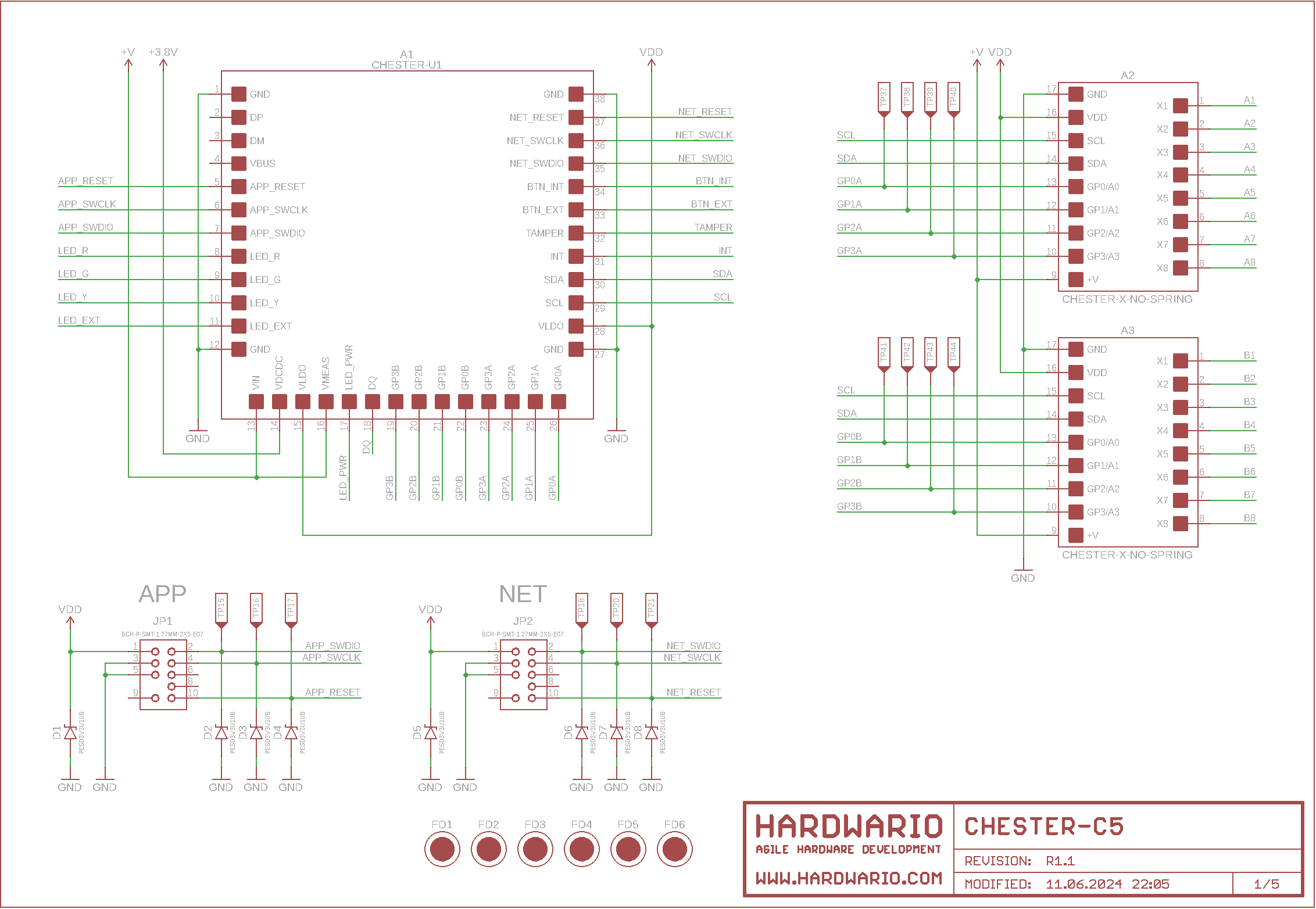
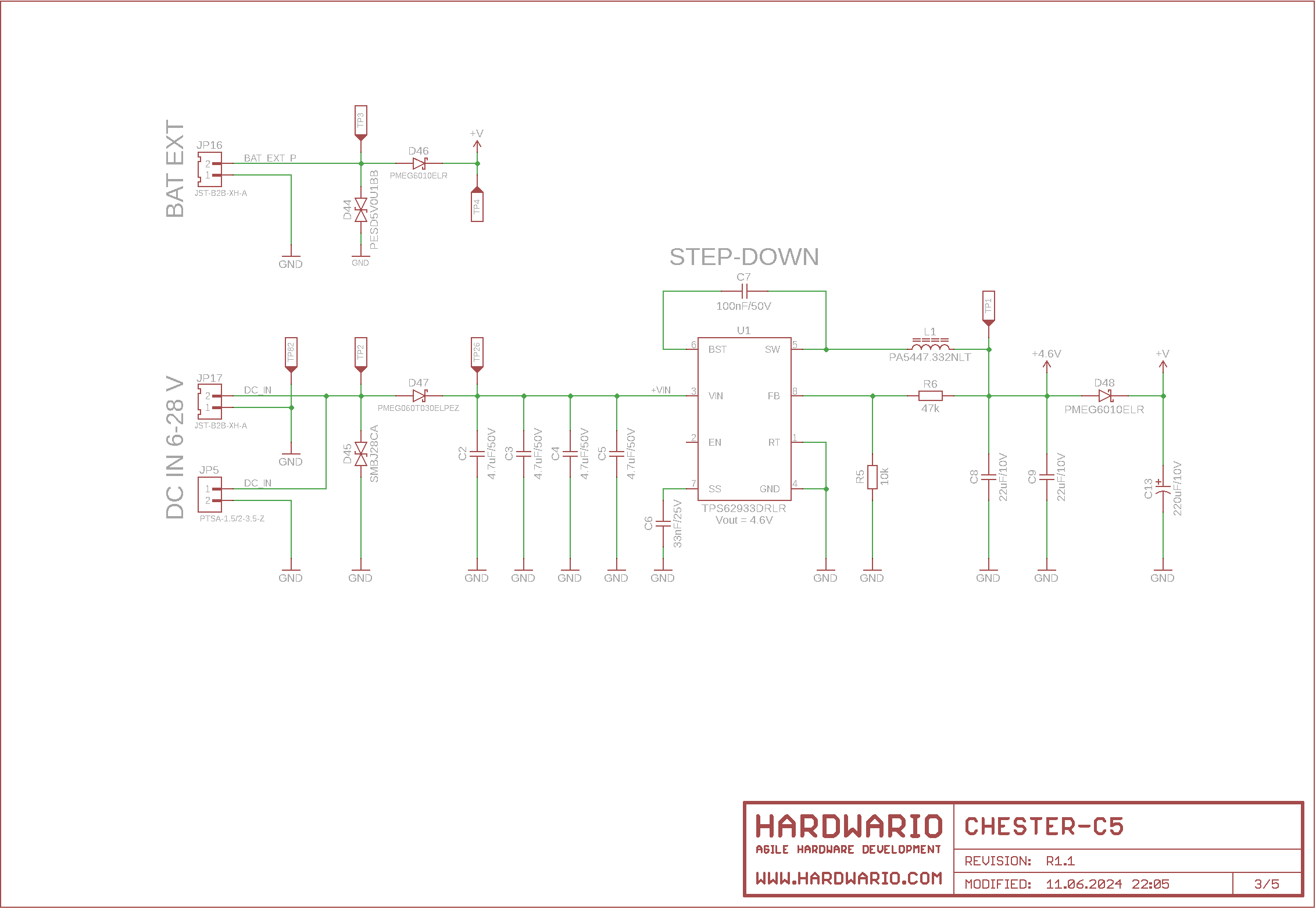
CHESTER-C5 is a custom carrier board for CHESTER-U1 designed as a NB-IoT / LTE-M gateway for connecting arrays of 1-Wire sensors (i.e. DS18B20) equipped with Lithium-Ion battery backup, implements a step-down DC/DC converter providing power from an external 6-28 VDC line (VIN) or 12V solar panel. It allows to measure input DC voltage, QWIIC interface can by used for connecting OLED display.
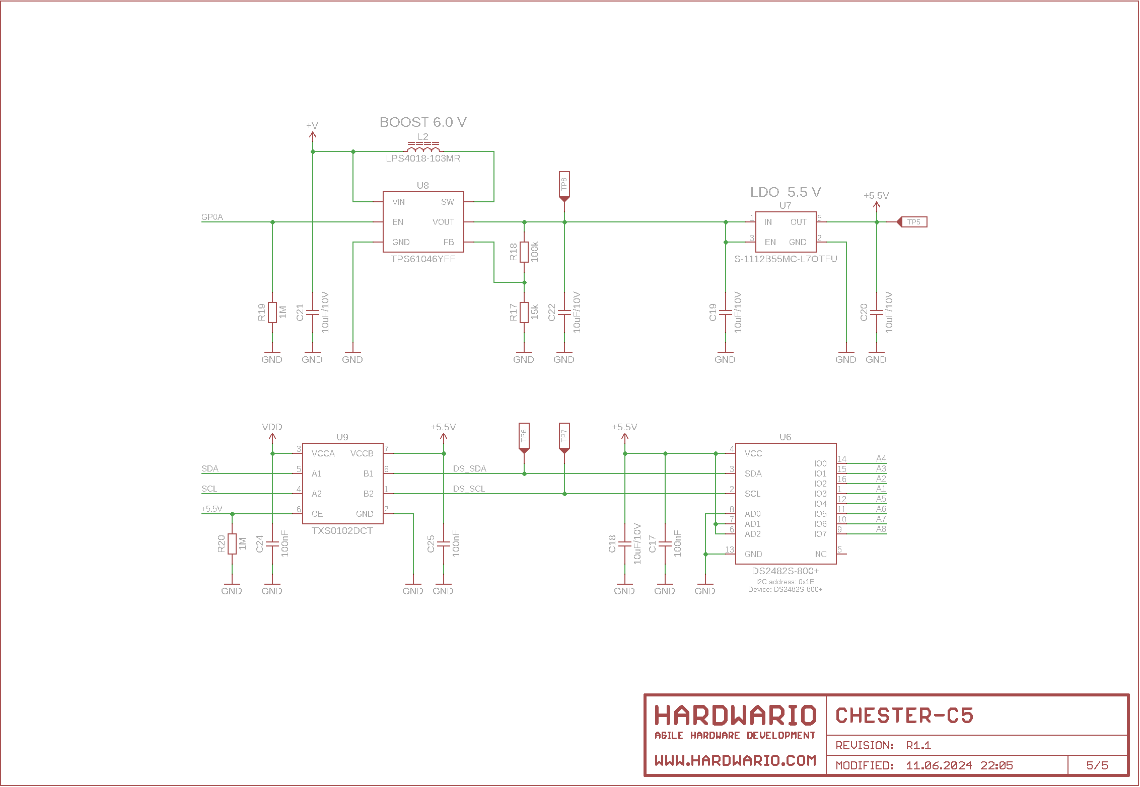
The board implements the Maxim DS2482S-800+ providing 8 independent 1-Wire channels on CHESTER-X slot A. Slot B can be extended with the CHESTER-X1 providing another 8-ch 1-Wire or any other CHESTER-X module.
CHESTER-C5 fits with the Polycase WH-04-02 enclosure.
Technical Specification
- Input DC voltage range (VIN): 6-28 VDC, suitable also for 12-18V solar panels*
- Nominal battery voltage: 3.7 V
- Battery charging current: 200 mA
- Battery idle current consumption <10 μA (without CHESTER-M)
- Recommended battery type for outdoor use: Samsung ICR18650-22P**
- Operating temperature: -40 to +70°C (without Li-Ion Battery)
- Storage temperature: -40 to +85°C (without Li-Ion Battery)
*Optimal photovoltaic solar panel for CHESTER: 12 V / 10 W
**Appropriate for solar panel application, charging temperature range -20 to +45°C, discharging -20 to +70°C
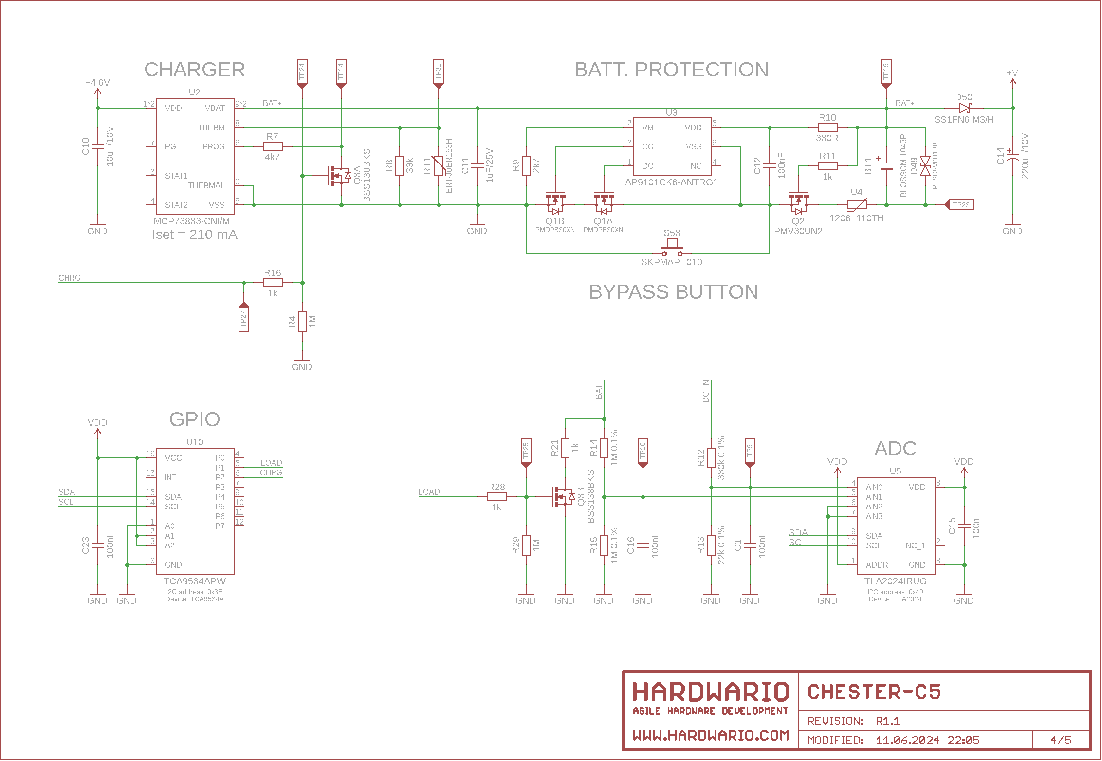
Battery charger and protection circuit
CHESTER-C5 implements the MCP73833 charger IC and the AP9101C protection IC protecting the battery by detecting overcharge voltage, overdischarge voltage, overcharge/discharge current.
For initial start powering from the battery without DC input power supply** it is necessary to long pres the Bypass button (BYPASS)**.
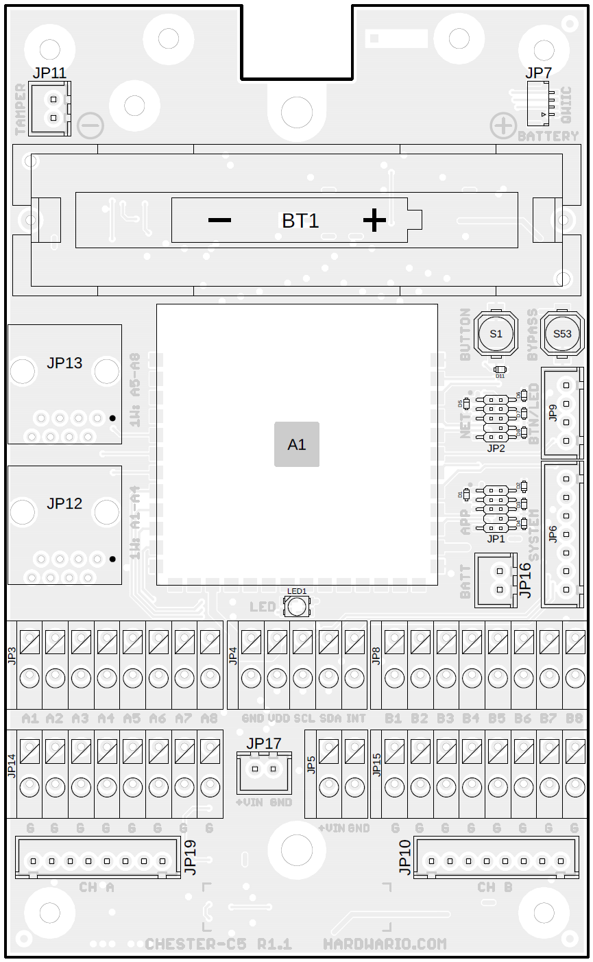
Module drawing: top
Module drawing: bottom
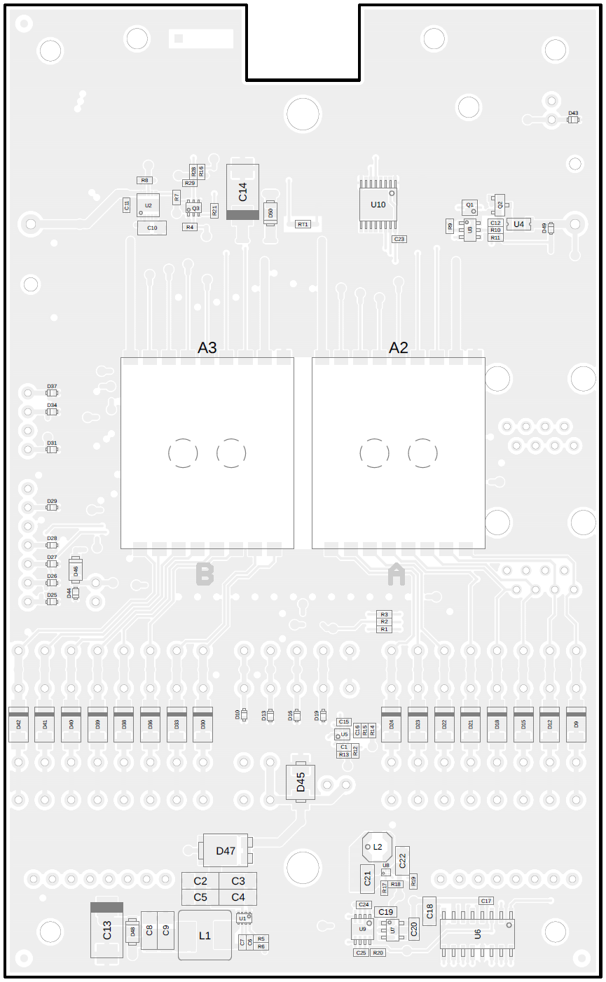
Module drawing description
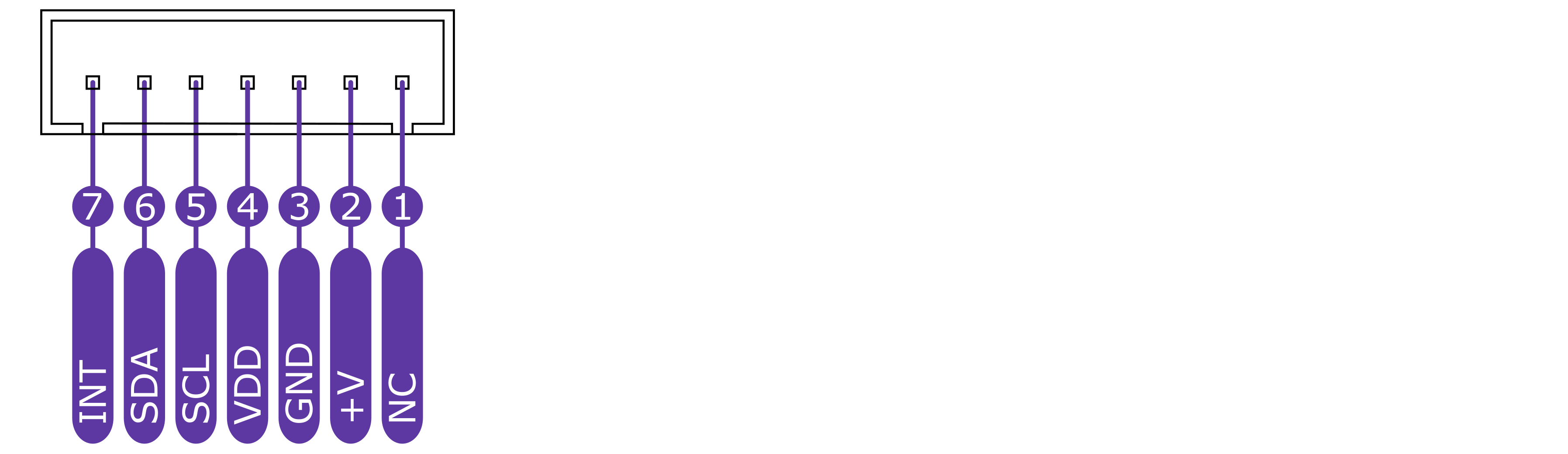
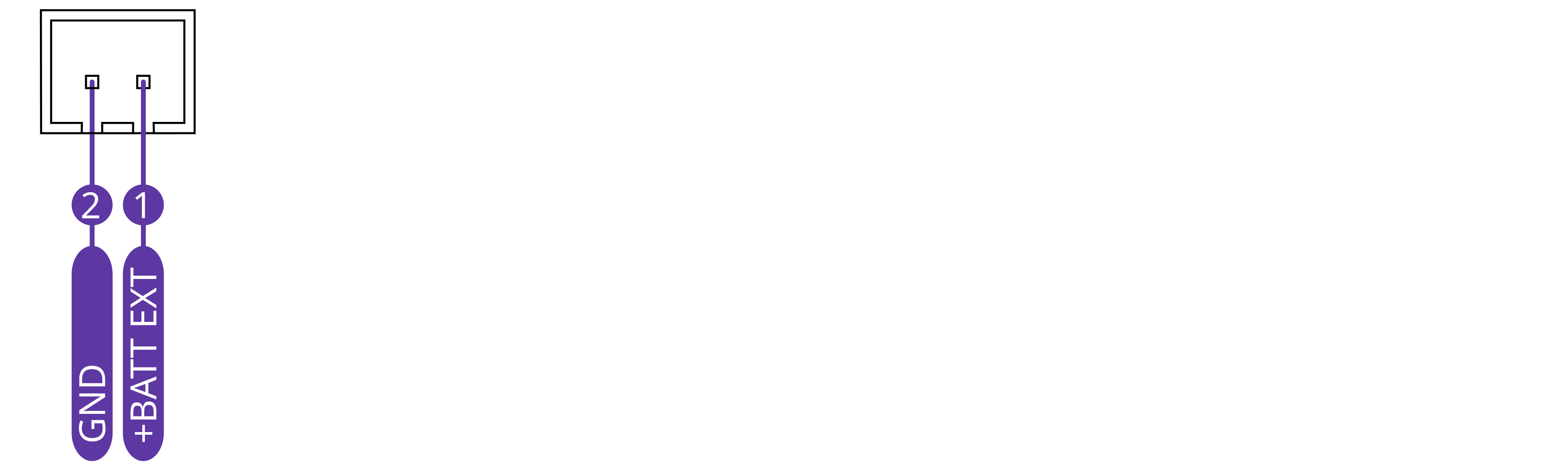
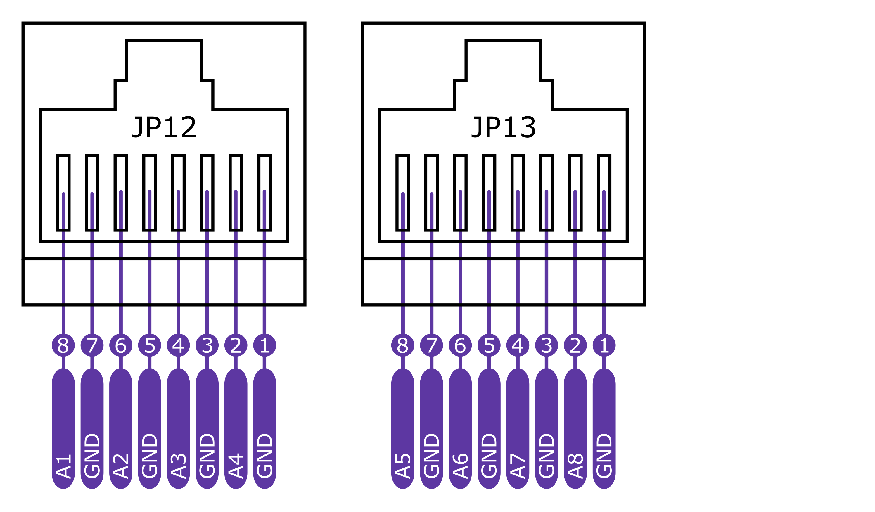
| Position | Name | Signal Description |
|---|---|---|
| A1 | CHESTER-U1 | CHESTER-U1 soldering slot |
| A2 | CHESTER-X A | CHESTER-X soldering slot A* |
| A2 | CHESTER-X B | CHESTER-X soldering slot B |
| A3 | CHESTER-U1 | CHESTER-U1 soldering slot |
| BT1 | BATTERY | 18650 Li-Ion battery holder |
| JP1 | APP SWD | Application MCU SWD / debug connector |
| JP2 | NET SWD | LTE Modem SWD / debug connector |
| JP3 | 1-Wire A | Integrated 8-ch 1-Wire interface terminal |
| JP4 | I2C | I2C interface terminal |
| JP5 | VIN | 6-28 V DC Power Input terminal |
| JP6 | SYSTEM | CHESTER SYSTEM JST connector |
| JP7 | QWIIC | QWIIC connector (i.e. for OLED) |
| JP8 | X slot B | CHESTER-X slot B terminal |
| JP9 | BT/LED | External Button + LED JST connector |
| JP10 | X slot B | CHESTER-X slot B JST con |
| JP11 | TAMPER | Tamper input (normally open) |
| JP12 | A1-A4 | 1-Wire A1-A4 + 4xGND RJ-45 con. |
| JP13 | A5-A8 | 1-Wire A1-A4 + 4xGND RJ-45 con. |
| JP14 | GND | Terminal with 8xGND |
| JP15 | GND | Terminal with 8xGND |
| JP16 | BATT | External battery or PPK input |
| JP17 | VIN | 6-28 V DC Power Input JST connector |
| JP19 | 1-Wire A | Integrated 8-ch 1-Wire interface JST con. |
| LED | RGY LED | RGY LED indication |
| S1 | BUTTON | CHESTER button |
| S53 | BYPASS | Battery protection bypass button** |
* CHESTER-X SLOT A is by default occupied with integrated module CHESTER-X1
** Use the BYPASS BUTTON to initiate start from the battery without DC input power
Pinout Description
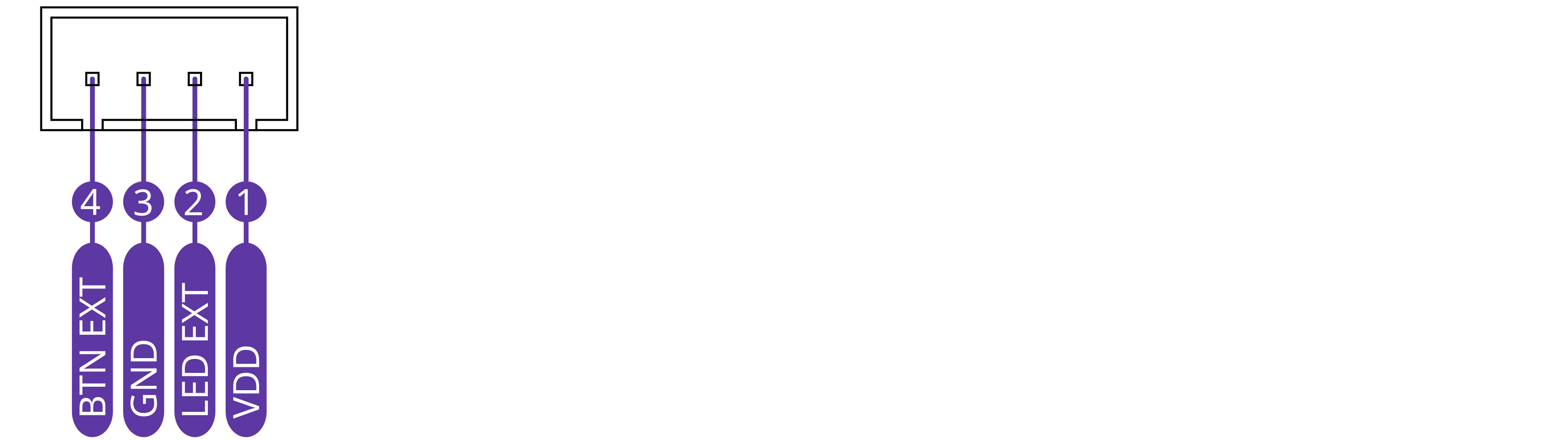
BT/LED Connector
SYSTEM Connector
BATTERY Connector
1-Wire RJ-45 Connectors
Schematic diagram
A schematic diagram is useful if you program low-level hardware-related code or if you're just curious about how the system is designed.