CHESTER-X0
This article describes the CHESTER-X0 four-channel I/O extension module. Two variants are available:
- CHESTER-X0A including 5.0V boost converter
- CHESTER-X0B without 5.0V boost converter
Module Overview
Each channel can be used for these applications:
- Digital input and output
- Analog input and output
- Voltage input 0 - 26 V*****
- Current loop 4 - 20 mA
- Dry contact input
- NPN and PNP input
- Power output
- X0A with boost converter: 5 V
- X0B w/o boost converter: standard 3.0 V (VDD solder bridge) or on request V+ battery rail (V+ solder bridge)
* CHESTER-M main board has on Ax and Bx terminal block pins TVS protection that starts to protect GPIO above 28 V. Theoretically you can measure higher voltage than 26 V but the protection distorts measurements or you need to request or remove these TVS.
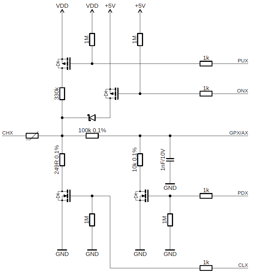
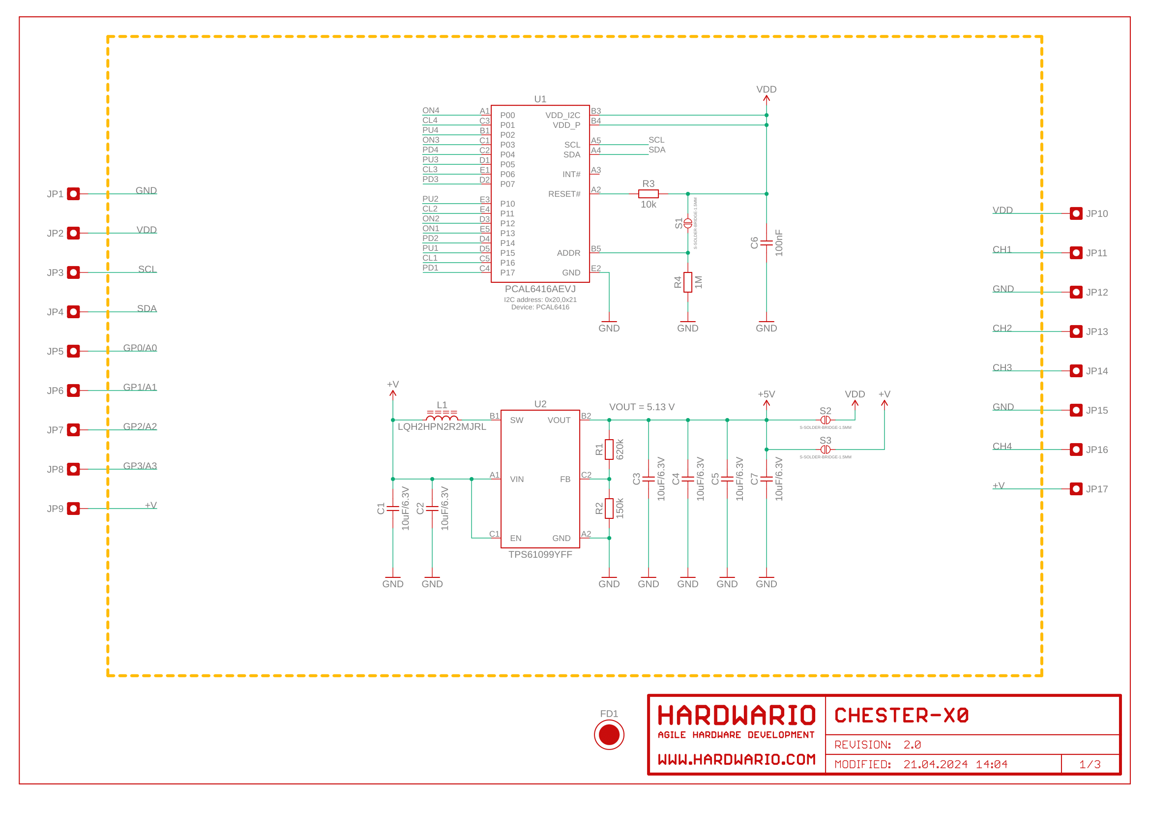
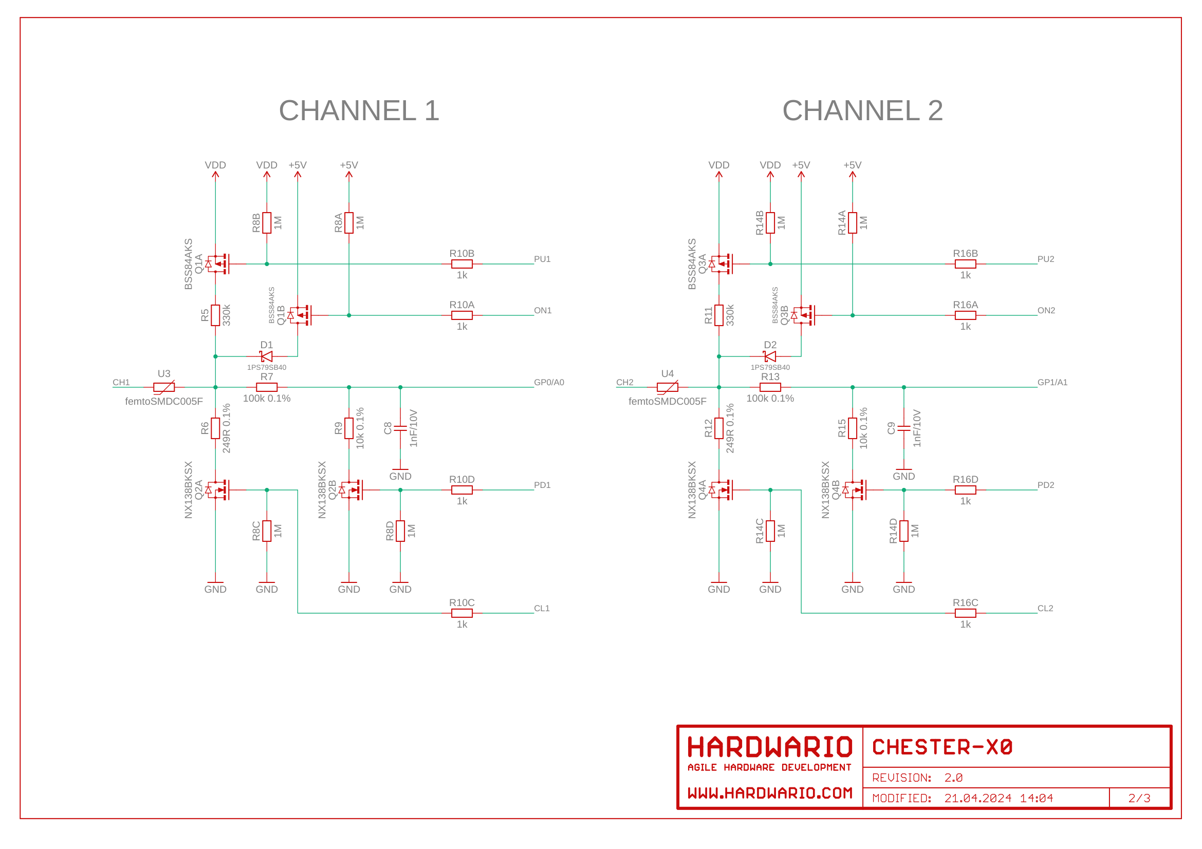
Channel Schematic Diagram
Depending on the application these configuration options are available for each channel:
- Enable pull-up resistor 330 kΩ (PUX)
- Enable pull-down resistor 249 Ω (PDX)
- Enable voltage divider (gain 1/11) (100 kΩ, 10 kΩ) (CLX)
- Enable 5V boost converter (CHESTER-X0A only) (ONX)
This picture show the electric circuit of each channel:
Configuration Table
The configuration depends on the application.
Signals PUx, CLx, PDx, ONx refers to the schematic above. Green tick ✅ means that the I2C GPIO expander or X0 sends a logic high signal to this configuration signal.
However, this is just to understand the modes. You only need to know which mode is set in the ctr_x0_set_mode table column.
| Application | PUx | CLx | PDx | ONx | SDK ctr_x0_set_mode |
|---|---|---|---|---|---|
| Analog input 0-26 V | ✅ | CTR_X0_MODE_AI_INPUT | |||
| Dry contact | ✅ | CTR_X0_MODE_DEFAULT | |||
| NPN input | ✅ | CTR_X0_MODE_NPN_INPUT | |||
| PNP input | ✅ | CTR_X0_MODE_PNP_INPUT | |||
| Current loop 4-20 mA | ✅ | ✅ | CTR_X0_MODE_CL_INPUT | ||
| Power source | ✅ | CTR_X0_MODE_PWR_SOURCE | |||
| Analog output 0-VDD | CTR_X0_MODE_DEFAULT | ||||
| Digital input | CTR_X0_MODE_DEFAULT | ||||
| Digital output | CTR_X0_MODE_DEFAULT |
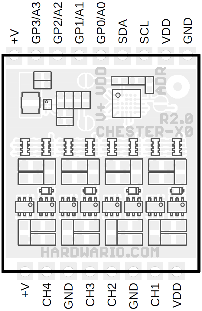
CHESTER Pin Configuration Diagram
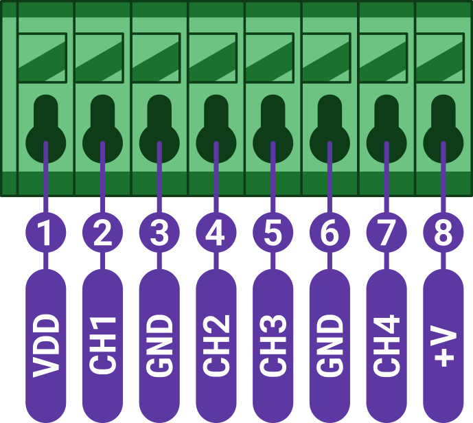
Pin Configuration and Functions
| Position | Signal Name | Signal Description |
|---|---|---|
| 1 | VDD | System VDD rail 3.0 V |
| 2 | CH1 | Channel 1 |
| 3 | GND | System ground signal |
| 4 | CH2 | Channel 2 |
| 5 | CH3 | Channel 3 |
| 6 | GND | System ground signal |
| 7 | CH4 | Channel 4 |
| 8 | +V | System positive rail (*) |
*Note: The system positive rail voltage depends on CHESTER power supply option.
Schematic diagram
A schematic diagram is useful if you program low-level hardware-related code or if you're just curious about how the system is designed.

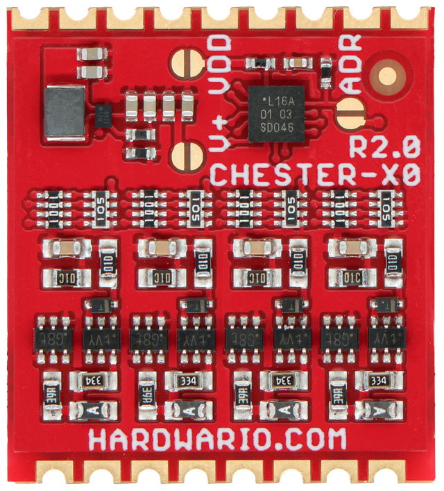
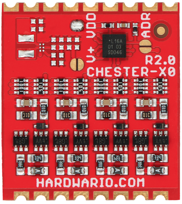
Module Drawing