CHESTER-M
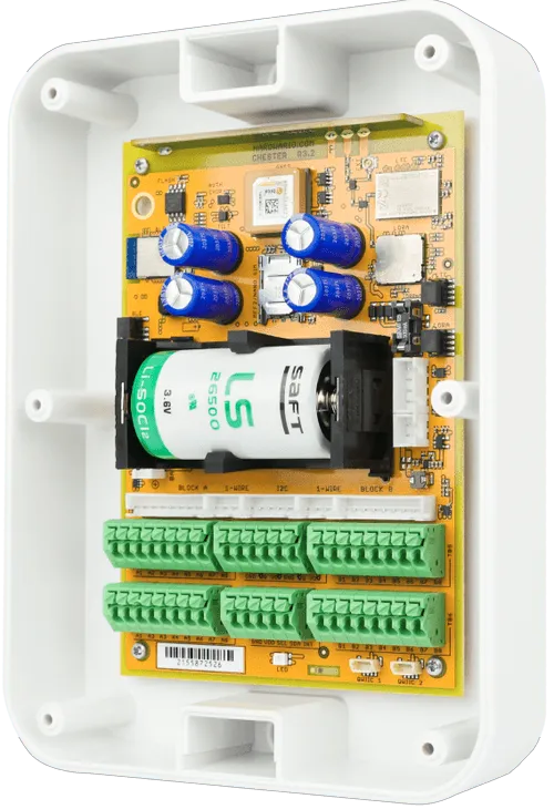
CHESTER-M is a versatile mainboard with LPWAN connectivity, extendable with X extension modules.
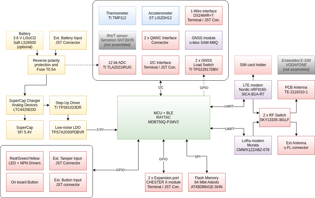
Block Diagram
Basic Parameters
This article provides basic parameters of the CHESTER platform:
| Name | Value | Remark |
|---|---|---|
| Operating voltage range | 2.0 to 5.25 V | For mainboard only, can be increased using extension modules |
| Typical idle current | 100 μA | Without any extension module and peripheral installed |
| Extra current for BLE | 50 μA | 1-second advertising interval |
| Extra current for NB-IoT/LTE-M | 100 μA | For ECL=0 and 30-minute transmission interval |
| Extra current for LoRaWAN | 50 μA | For SF12 and 30-minute transmission interval |
| Enclosure dimensions | 130(w) x 175(h) x 45(d) mm | Standard enclosure |
| Enclosure dimensions | 200(w) x 280(h) x 45(d) mm | Carrier board, low profile |
| Enclosure dimensions | 200(w) x 280(h) x 65(d) mm | Carrier board, high profile |
| Operating temperature range | -20 to +60 °C | |
| Storage temperature range | -30 to +70 °C | |
| Protection level | IP 67 | Can be immersed in 1 m depth for 30 minutes |
The parameters provided above might be affected by the specific hardware configuration and application implementation.
Connector Description
Terminal Blocks Description
The terminal block signals are defined by placing extension X modules on the backside of the CHESTER mainboard. You can find more information in the Backside Modules chapter.
Terminal Block Solder Bridges
When there are no extension modules in slot A or B, the 8-pin terminal blocks can be configured using solder bridges.
Terminal block pins can have these signals based on solder bridges:
- Terminals A1-A8 and B1-B8 can be connected to the GND.
- Terminals A6, A3, B6, B3 can be connected to VDD
- Terminals A5, A2, B5, B2 can be connected to DQ (1-Wire Bus).
1-Wire extension
This picture shows how to extend the 1-Wire bus to 8-pin terminal blocks A and B. Solder the highlighted solder bridges so the 1-Wire signals from the 1-Wire terminal block are duplicated to the 8-pin terminal blocks.
Please note that the solder bridges are on the bottom side of the PCB. So in the picture below the blue solder bridge rectangles on the right of the PCB actually connects signals to the left 8-pin terminal blocks TB1 and TB2 when looked at the front of the PCB.
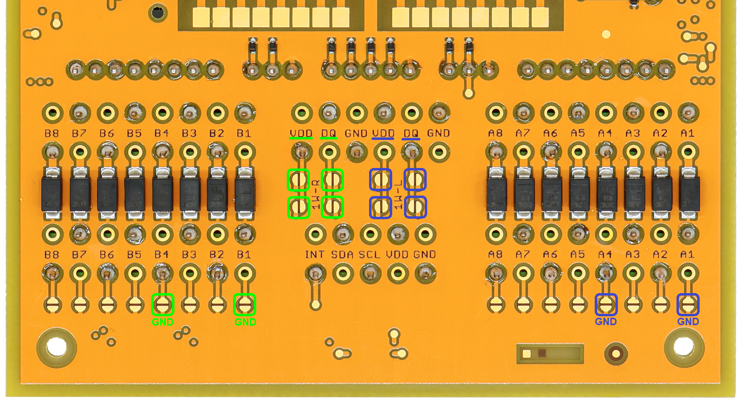
This picture shows the terminal blocks connection:
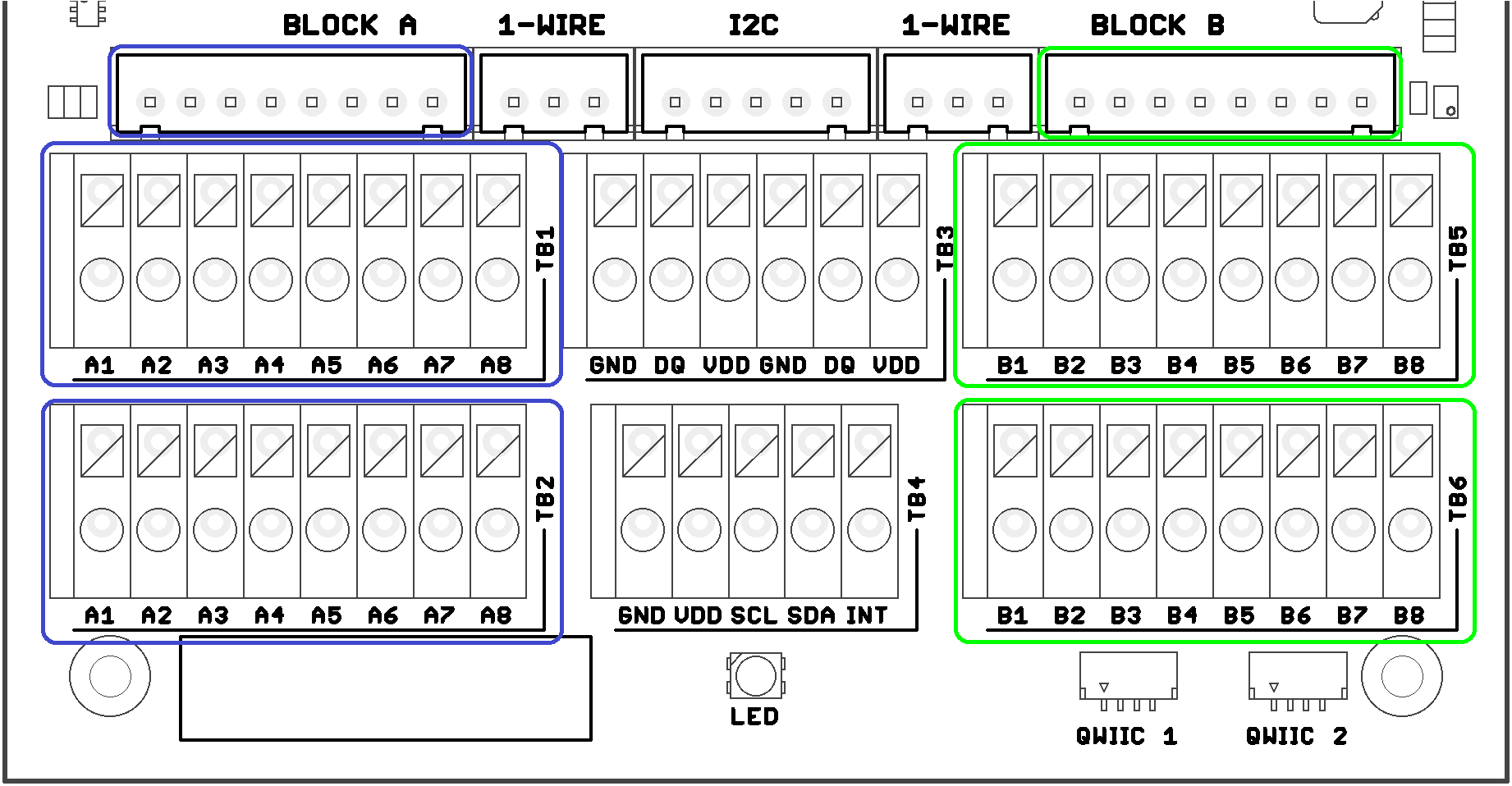
This table shows the connection of 1-Wire to terminal blocks and JST 8-pin connectors::
| Terminal BLOCK Position | Signal Name | Signal Description |
|---|---|---|
| A1 or B1 | GND | System ground signal |
| A2 or B2 | DQ | 1-Wire Data |
| A3 or B3 | VDD | Power |
| A4 or B4 | GND | System ground signal |
| A5 or B5 | DQ | 1-Wire Data |
| A6 or B6 | VDD | Power |
| A7 or B7 | NC or GND | Not connected or GND |
| A8 or B8 | NC or GND | Not connected or GND |
Backside Module
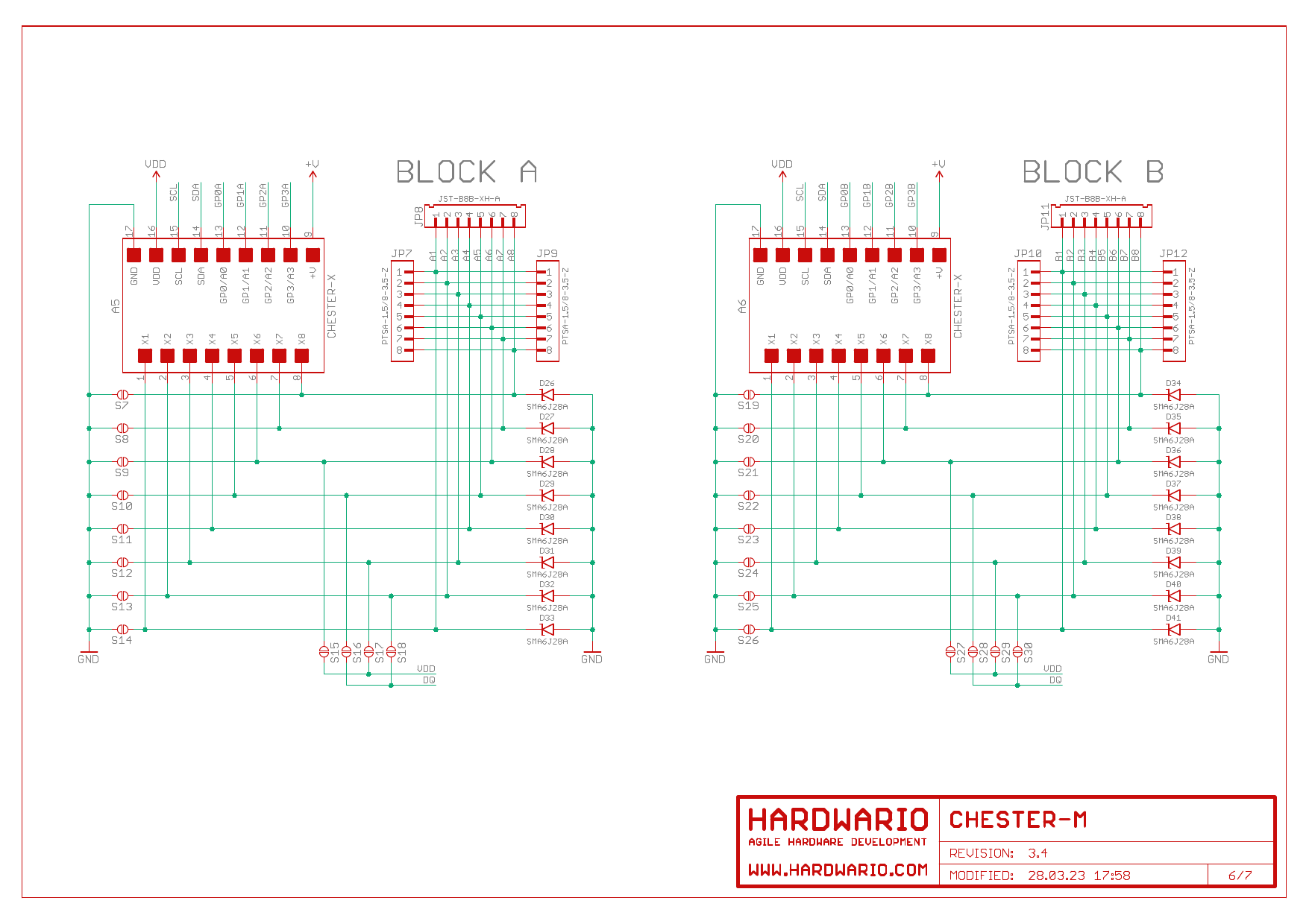
This section provides information on signal mapping for the two backside slots (A and B) on the CHESTER mainboard.
The backside slots use two rows of signals:
-
Top Row (closer to the antenna)
This signal row (with nine 2.54 mm distanced pins) provides power rails + digital signals with the signal definition in the table below.
-
Bottom Row (closer to the terminal blocks)
This signal row (with eight 2.54 mm distanced pins) directly connects to the terminal blocks, and their meaning is module-specific.
Top Row Signals (Slot A)
The following table lists the signals in the left-to-right order when you flip the board (slot A is on the right side).
| Position | Signal Name | Signal Description | Connection on nRF52840 |
|---|---|---|---|
| 1 | +V | System positive rail | - |
| 2 | GP3A | General purpose I/O | P0.31/AIN7 |
| 3 | GP2A | General purpose I/O | P0.02/AIN0 |
| 4 | GP1A | General purpose I/O | P0.29/AIN5 |
| 5 | GP0A | General purpose I/O | P0.03/AIN1 |
| 6 | SDA | System I²C bus (data) | - |
| 7 | SCL | System I²C bus (clock) | - |
| 8 | VDD | System VDD rail | - |
| 9 | GND | System ground signal | - |
Top Row Signals (Slot B)
The following table lists the signals in the left-to-right order when you flip the board (slot B is on the left side).
| Position | Signal Name | Signal Description | Connection on nRF52840 |
|---|---|---|---|
| 1 | +V | System positive rail | - |
| 2 | GP3B | General purpose I/O | P0.05/AIN3 |
| 3 | GP2B | General purpose I/O | P0.04/AIN2 |
| 4 | GP1B | General purpose I/O | P0.30/AIN6 |
| 5 | GP0B | General purpose I/O | P0.28/AIN4 |
| 6 | SDA | System I²C bus (data) | - |
| 7 | SCL | System I²C bus (clock) | - |
| 8 | VDD | System VDD rail | - |
| 9 | GND | System ground signal | - |
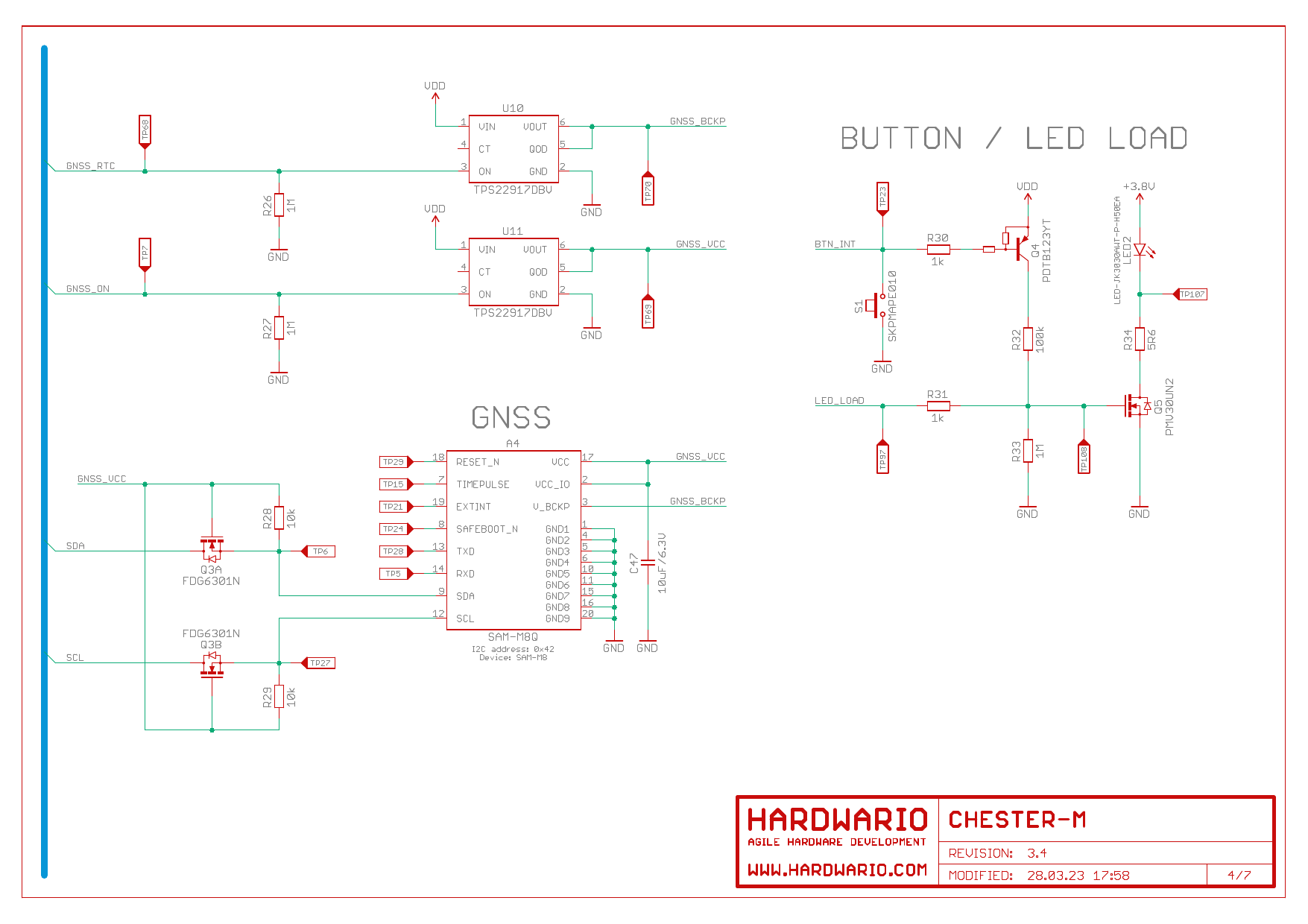
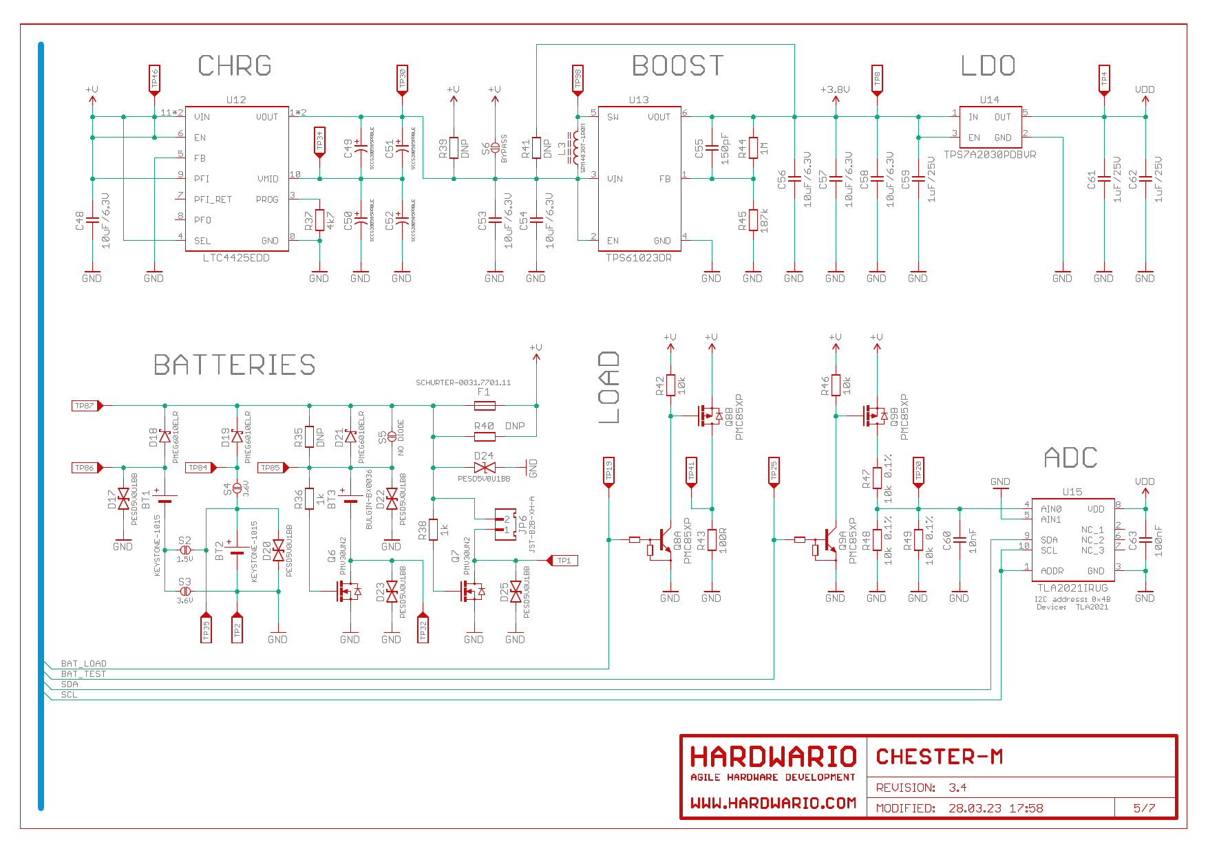
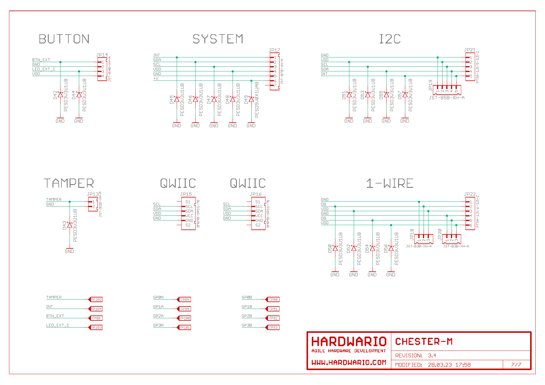
Schematic Diagram
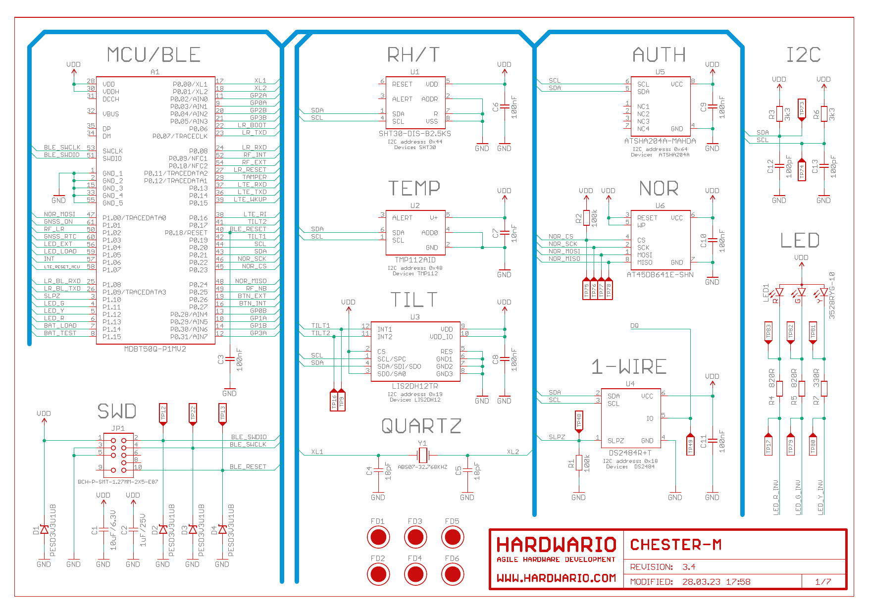
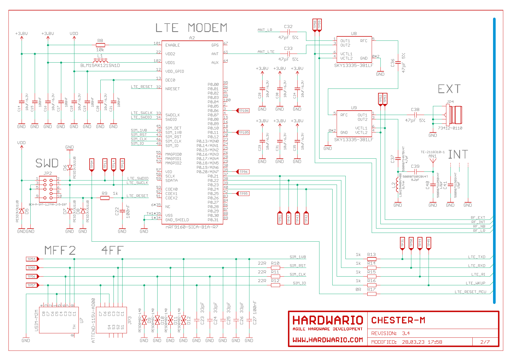
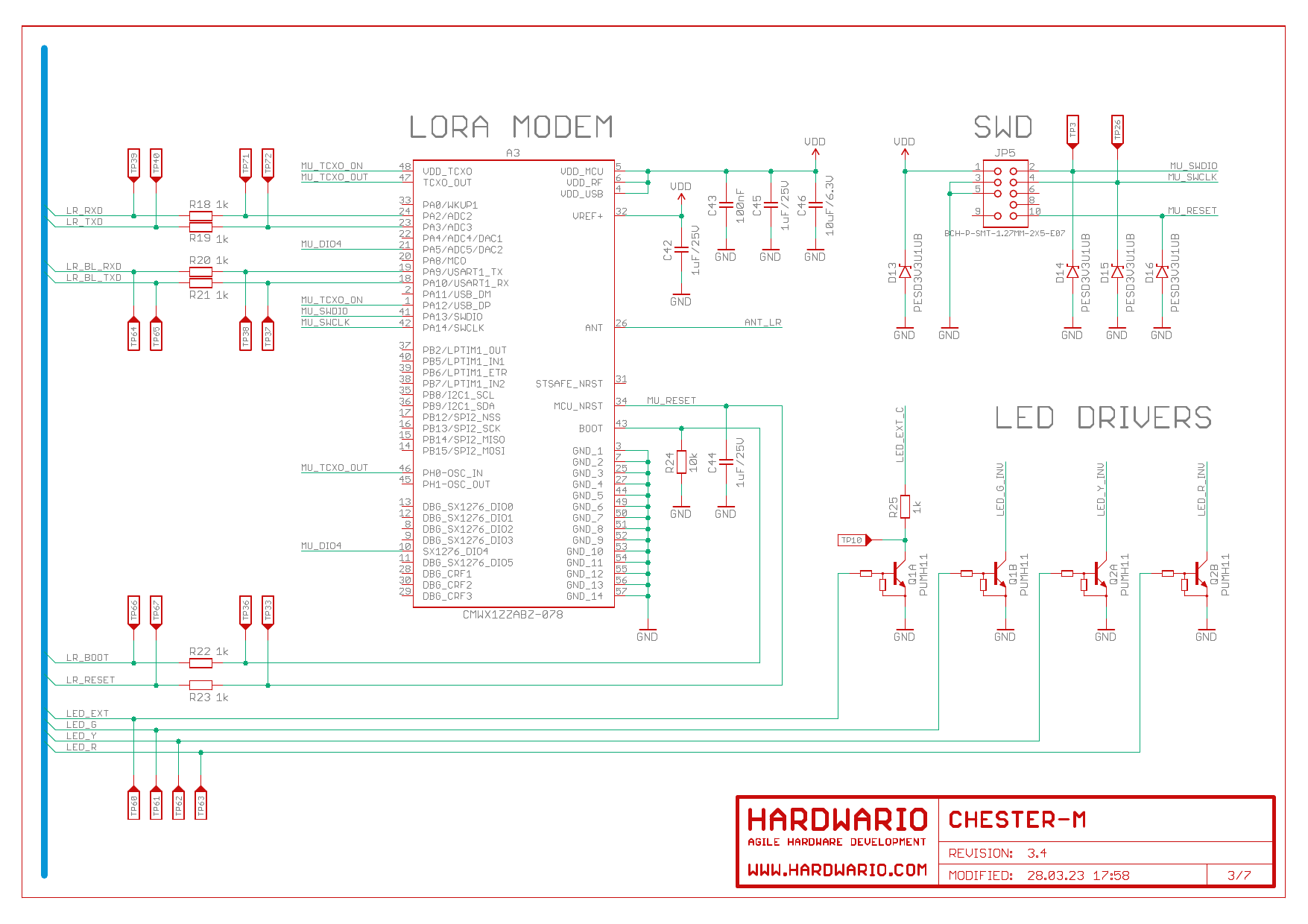
A schematic diagram is useful if you program low-level hardware-related code or if you're just curious about how the system is designed.
MCU
LTE
LoRaWAN
GNSS
Power
Terminals
Nets
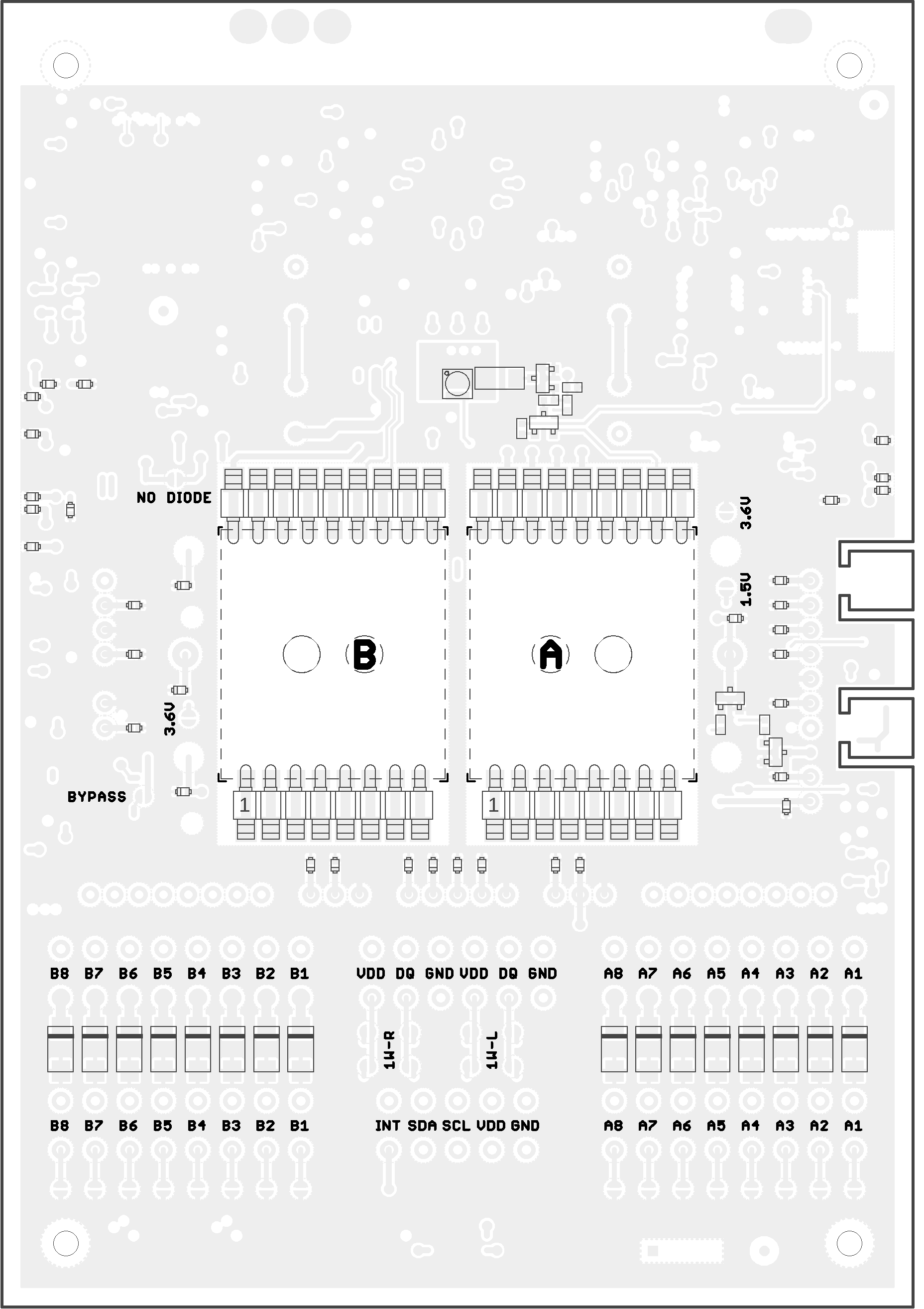
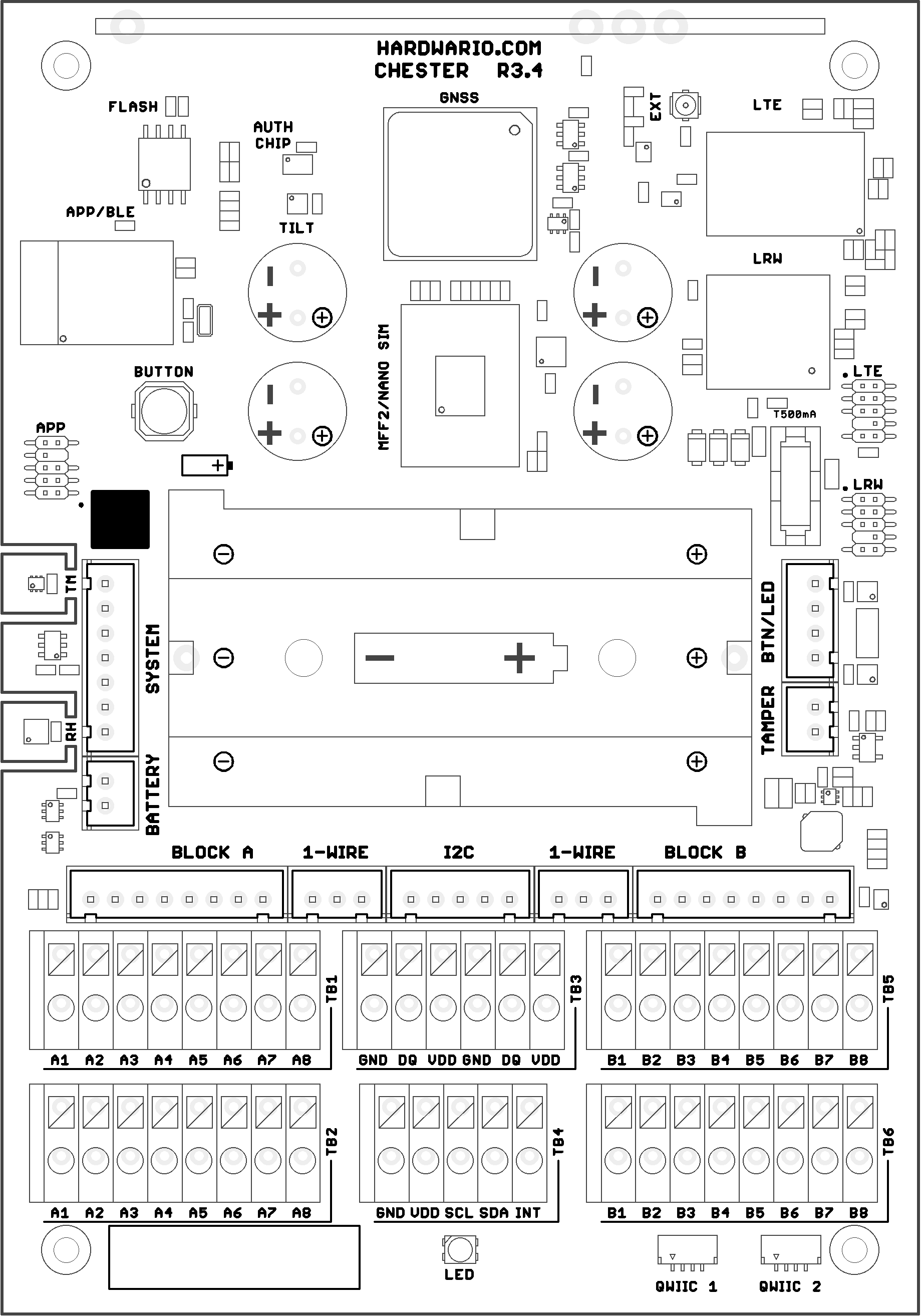
Layout Placement
Top
Bottom