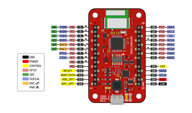
Header Pinout
The TOWER Kit emphasizes hardware modularity and reusability. To achieve such a goal, the proper interconnection system has to be used.
TOWER sticks to a well-known and widely accepted standard - the so-called headers with a 2.54 mm (0.1 inches) pitch.
Core Module pinout
You can visit the separate chapter to learn more About Core Module.
Eagle Footprint Library
You can download the TOWER library for Eagle EDA software which contains Standard Module and Cloony format.
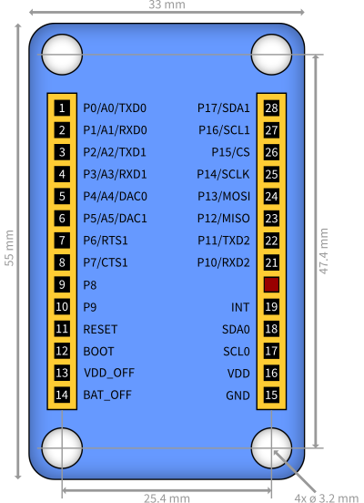
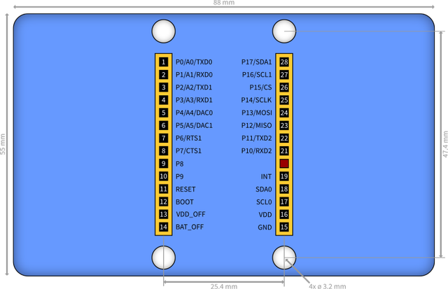
Module Drawing And Pinout
Module Format
Format Module defines
- Spacing and signals between two rows of 14-pin headers
- Four mounting hole positions and their diameter
- Position of mechanical key (filled hole in the header) preventing reverse insertion
- Position of sockets from the top view
- Position of pins from the bottom view
- Recommended PCB height 55 mm
- Recommended PCB thickness 1.5 mm
- The radius of rounded corners 3.8 mm
Standard Module
Large Module
Module Signals
This is a summary of basic peripherals available on the module header
- 18x GPIO channels (General Purpose Input/Output)
- 6x ADC channels (Analog-to-Digital Converter)
- 2x DAC channels (Digital-to-Analog Converter)
- 3x UART channels (Universal Asynchronous Receiver Transmitter)
- 2x I²C bus (Inter-Integrated Circuit)
- 1x SPI bus (Serial Peripheral Interface)
The following table defines signal assignment on the module header
| Pin | Signal | Description | STM32 GPIO |
|---|---|---|---|
| 1 | P0 A0 TXD0 | GPIO channel 0 ADC channel 0 UART channel 0 - TXD signal | PA0 |
| 2 | P1 A1 RXD0 | GPIO channel 1 ADC channel 1 UART channel 0 - RXD signal | PA1 |
| 3 | P2 A2 TXD1 | GPIO channel 2 ADC channel 2 UART channel 1 - TXD signal | PA2 |
| 4 | P3 A3 RXD1 | GPIO channel 3 ADC channel 3 UART channel 1 - RXD signal | PA3 |
| 5 | P4 A4 DAC0 A | GPIO channel 4 ADC channel 4 DAC channel 0 Sensor Module Channel A | PA4 |
| 6 | P5 A5 DAC1 B | GPIO channel 5 ADC channel 5 DAC channel 1 Sensor Module Channel B | PA5 |
| 7 | P6 RST1 | GPIO channel 6 UART channel 1 - RTS signal | PB1 |
| 8 | P7 A6 CTS1 C | GPIO channel 7 ADC channel 6 UART channel 1 - CTS signal Sensor Module Channel C | PA6 |
| 9 | P8 | GPIO channel 8 | PB0 |
| 10 | P9 | GPIO channel 9 | PB2 |
| 11 | RESET | System reset | NRST |
| 12 | BOOT | Boot mode | BOOT0 |
| 13 | VDD_OFF | From top side: VDD_OFF_OUT From bottom side: VDD_OFF_IN | |
| 14 | BAT_OFF | Battery disconnect signal | |
| 15 | GND | System GND (ground) | |
| 16 | VDD | System VDD (positive rail) | |
| 17 | SCL0 | I²C bus 0 - SCL signal | PB10 |
| 18 | SDA0 | I²C bus 0 - SDA signal | PB11 |
| 19 | INT | System interrupt signal | PC13 |
| 20 | Key - no signal | ||
| 21 | P10 RXD2 | UART channel 2 - RXD signal | PA10 |
| 22 | P11 TXD2 | UART channel 2 - TXD signal | PA9 |
| 23 | P12 MISO | SPI bus - MISO signal | PB14 |
| 24 | P13 MOSI | SPI bus - MOSI signal | PB15 |
| 25 | P14 SCLK | SPI bus - SCLK signal | PB13 |
| 26 | P15 CS | SPI bus - CS signal | PB12 |
| 27 | P16 SCL1 | I²C bus 1 - SCL signal | PB8 |
| 28 | P17 SDA1 | I²C bus 1 - SDA signal | PB9 |
Do not connect anything on the VDD_OFF and BAT_OFF signals unless you are sure what you are doing.
Tag Drawing And Pinout
Tag Format
The primary purpose of tag format is to provide signal break-out for I²C peripheral in a compact form factor. It can be anything I²C-related - e.g. sensors, memories, RTCs, etc.
Format Tag defines
- Signals on a 5-pin header (see table below)
- Letter “D”-shaped PCB outline
- Mechanical dimensions 16 x 16 mm
- Recommended PCB thickness 1.5 mm
- The radius of rounded corners 3.8 mm
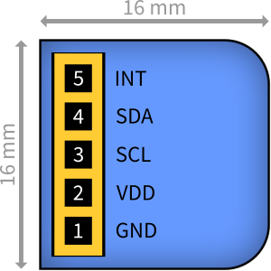
Tag Signals
The following table defines signal assignment on the tag header:
| Pin | Signal | Description |
|---|---|---|
| 1 | GND | System GND (ground) |
| 2 | VDD | System VDD (positive rail) |
| 3 | SCL | I²C bus - SCL signal |
| 4 | SDA | I²C bus - SDA signal |
| 5 | INT | System interrupt signal |